
SiC MOSFET device low-temperature stability evaluation test method

A test method and stability technology, applied in the field of reliability testing of silicon carbide semiconductor devices, can solve the problem of not specifying the test method for evaluating the stability of the device, etc.

Active Publication Date: 2019-01-25
DALIAN UNIV OF TECH
View PDF9 Cites 5 Cited by
  • Summary
  • Abstract
  • Description
  • Claims
  • Application Information

AI Technical Summary

Problems solved by technology

However, the patent applicant did not specify the test method for evaluating the stability of the device

Method used


Image

  • SiC MOSFET device low-temperature stability evaluation test method
  • SiC MOSFET device low-temperature stability evaluation test method
  • SiC MOSFET device low-temperature stability evaluation test method

Examples


Embodiment 1

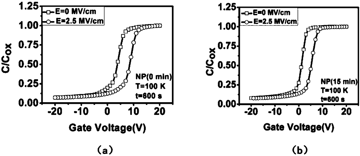
[0031] Introduce nitrogen gas into the chamber of the probe station, open the chamber after 5 minutes and put in MOSFET samples made of 2 silicon carbide wafers that have been processed by ECR nitrogen plasma passivation for 0min and 15min, close the chamber, and close the chamber. Nitrogen cylinder; turn on the mechanical pump to evacuate until it reaches 10 -4When Pa is below, turn off the chamber knob, turn off the mechanical pump, and use liquid nitrogen to lower the chamber to a low temperature of 100K; at a low temperature test temperature of 100K, use the 4200-SCS semiconductor parameter tester to measure high-frequency C-V curves and semiconductor parameters. The instrument frequency is set to 1MHz, and the scanning voltage is -20V to 20V; after measuring the high-frequency C-V curve at 100K, a positive electric field stress of 2.5MV / cm is applied in situ for 600s, and the C-V curve is measured again immediately after the positive electric field stress ends ; Calculate...

Embodiment 2

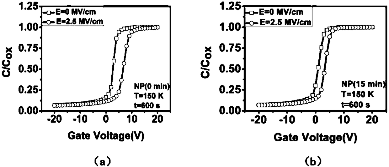
[0036] Introduce nitrogen gas into the chamber of the probe station, open the chamber after 5 minutes and put in MOSFET samples made of 2 silicon carbide wafers that have been processed by ECR nitrogen plasma passivation for 0min and 15min, close the chamber, and close the chamber. Nitrogen cylinder; turn on the mechanical pump to evacuate until it reaches 10 -4 When Pa is below, close the chamber knob, turn off the mechanical pump, and use liquid nitrogen to lower the chamber to a low temperature of 150K; at a low temperature test temperature of 150K, use a 4200-SCS semiconductor parameter tester for high-frequency C-V curve measurement, semiconductor parameter tester The frequency is set to 1MHz, and the scanning voltage is -20V to 20V; after measuring the high-frequency C-V curve at 150K, a positive electric field stress of 2.5MV / cm is applied in situ for 600s, and the C-V curve is measured again immediately after the stress is over; The drift of the C-V curve before and af...

Embodiment 3

[0041] Introduce nitrogen gas into the chamber of the probe station, open the chamber after 5 minutes and put in MOSFET samples made of 2 silicon carbide wafers that have been processed by ECR nitrogen plasma passivation for 0min and 15min, close the chamber, and close the chamber. Nitrogen cylinder; turn on the mechanical pump to evacuate until it reaches 10 -4 When Pa is below, close the chamber knob, turn off the mechanical pump, and use liquid nitrogen to lower the chamber to a low temperature of 200K; at a low temperature test temperature of 200K, use a 4200-SCS semiconductor parameter tester for high-frequency C-V curve measurement, semiconductor parameter tester The frequency is set to 1MHz, and the scanning voltage is -20V to 20V; after measuring the high-frequency C-V curve at 200K, a positive electric field stress of 2.5MV / cm is applied in situ for 600s, and the C-V curve is measured again immediately after the positive electric field stress ends; Calculate the ΔV by...


PUM


Abstract

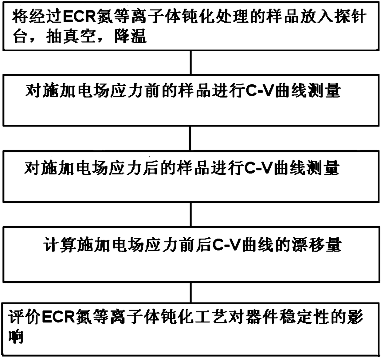
The invention belongs to the technical field of silicon carbide semiconductor device reliability test and relates to a SiC MOSFET device low-temperature stability evaluation test method. The method includes the following steps that: (1) a sample subjected to ECR nitrogen plasma passivation treatment is arranged into a probe station so as to be subjected to vacuumization and cooling; (2) C-V curvemeasurement is performed on the sample which has not been subjected to electric field stress; (3) C-V curve measurement is performed on the sample which has been subjected to electric field stress; (4) the drift quantity of a C-V curve before and after the application of the electric field stress is calculated; and (5) the influence of an ECR nitrogen plasma passivation process on device stabilityis evaluated. With the method of the invention adopted, the influence of movable charges and fixed charges on the stability of a SiC MOSTET device at low-temperature (80-300K) measurement can be eliminated; the separate passivation effects of the passivation process for an oxide layer trap and an interface trap are explored; and the charge number of the oxide layer trap and the charge number of the interface trap of the sample are calculated; and the low-temperature stability of the SiC MOSFET device can be evaluated.

Description

technical field [0001] The invention relates to a method for evaluating and testing the low-temperature stability of SiC MOSFET devices, and belongs to the technical field of reliability testing of silicon carbide semiconductor devices. Background technique [0002] SiC semiconductors are widely used in harsh environments such as high temperature, high frequency and high voltage because of their advantages such as high carrier drift speed, large bandgap width, and strong critical breakdown electric field, and because SiC semiconductors are the only ones that can directly heat Oxidation to form SiO 2 Thin-film wide bandgap compound semiconductors, so it is the best choice to replace traditional silicon to manufacture SiC MOS devices. However, in the actual oxidation and subsequent steps, there will be a large number of traps and charges in the oxide layer of SiC MOS devices, which will cause a serious shift in the flat band voltage of the C-V curve (MOSFET threshold voltage)...

Claims


Application Information

Patent Timeline
IPC IPC(8): G01R31/26
CPCG01R31/2642
Inventor 王德君孙雨浓杨超秦福文
Owner DALIAN UNIV OF TECH
Learn More