System and method for detecting non-defective products of integrated circuits

A technology of integrated circuit and detection system, which is applied in the field of intelligent, efficient, multi-chip and less-channel test system and integrated circuit good product detection system, which can solve the problems of reducing the inconvenience of test items, occupying circuit area, and high cost of ATE test, so as to shorten the test time. Time, the effect of improving test efficiency

Active Publication Date: 2019-01-29
UNIV OF ELECTRONICS SCI & TECH OF CHINA
View PDF6 Cites 2 Cited by
  • Summary
  • Abstract
  • Description
  • Claims
  • Application Information

AI Technical Summary

Problems solved by technology

[0004] DFT technology is to implant some special structures into the circuit during the design stage, so that the test can be performed after the design is completed; by adding testability design structures, such as scan chains, BIST (build-in-self-test), etc., internal signals can be exposed to Outside the circuit; such as: BIST testing technology is widely used in the semiconductor industry. The BIST technology used in the memory includes implanting the test pattern generation circuit, sequential circuit, mode selection circuit and debugging test circuit in the circuit. However, implanting BIST in the chip will cause Occupies additional circuit area, additional pins, increases chip cost, and may have test blind spots
[0005] ATE (Automatic Test Equipment) uses MCU, PLC, PC based on VB, VC development platform, uses Test Stand&LabVIEW and JTAG / Boundary Scan and other technologies to develop and design various types of automated test equipment according to customer's test requirements, drawings and reference schemes; The cost of ATE testing is extremely high, and the test items need to be negotiated with the test factory, so it is extremely inconvenient to increase or decrease the test items

Method used


Image

  • System and method for detecting non-defective products of integrated circuits
  • System and method for detecting non-defective products of integrated circuits
  • System and method for detecting non-defective products of integrated circuits

Examples


Embodiment Construction

[0028] The present invention will be further described below in conjunction with the accompanying drawings.

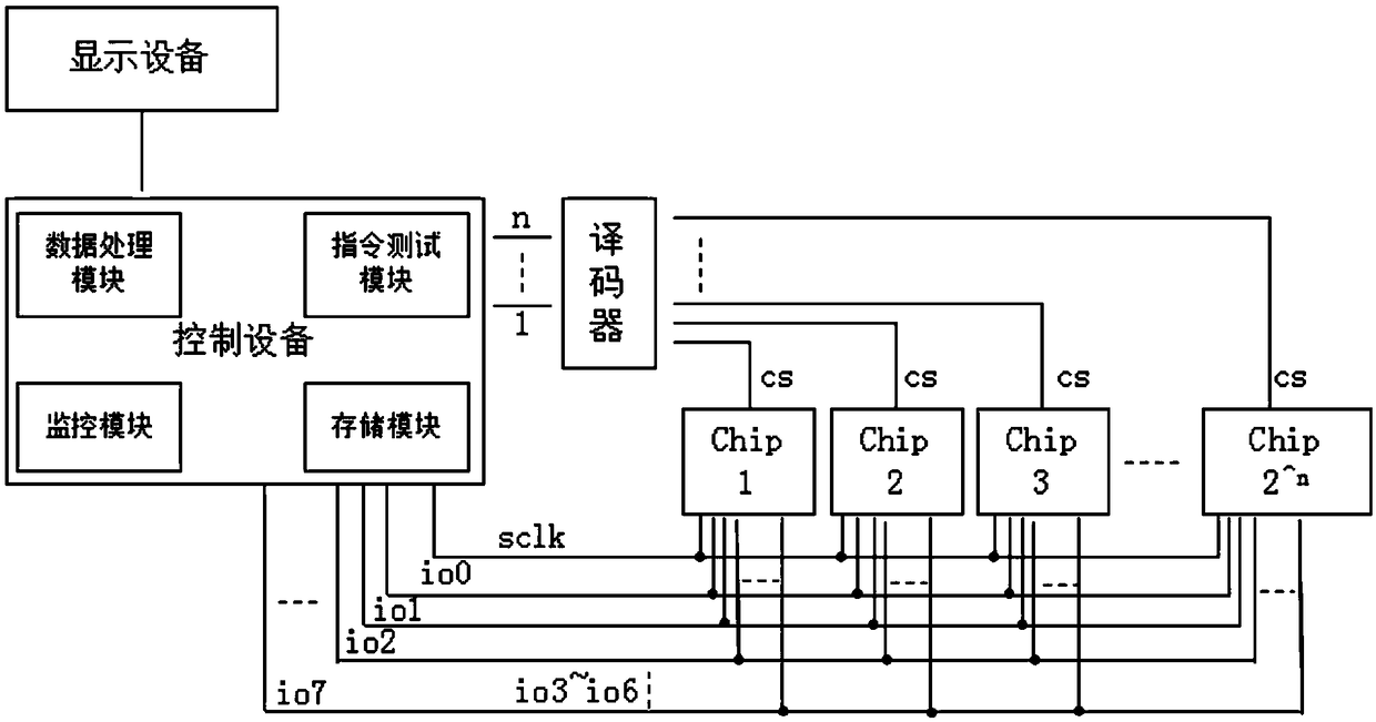
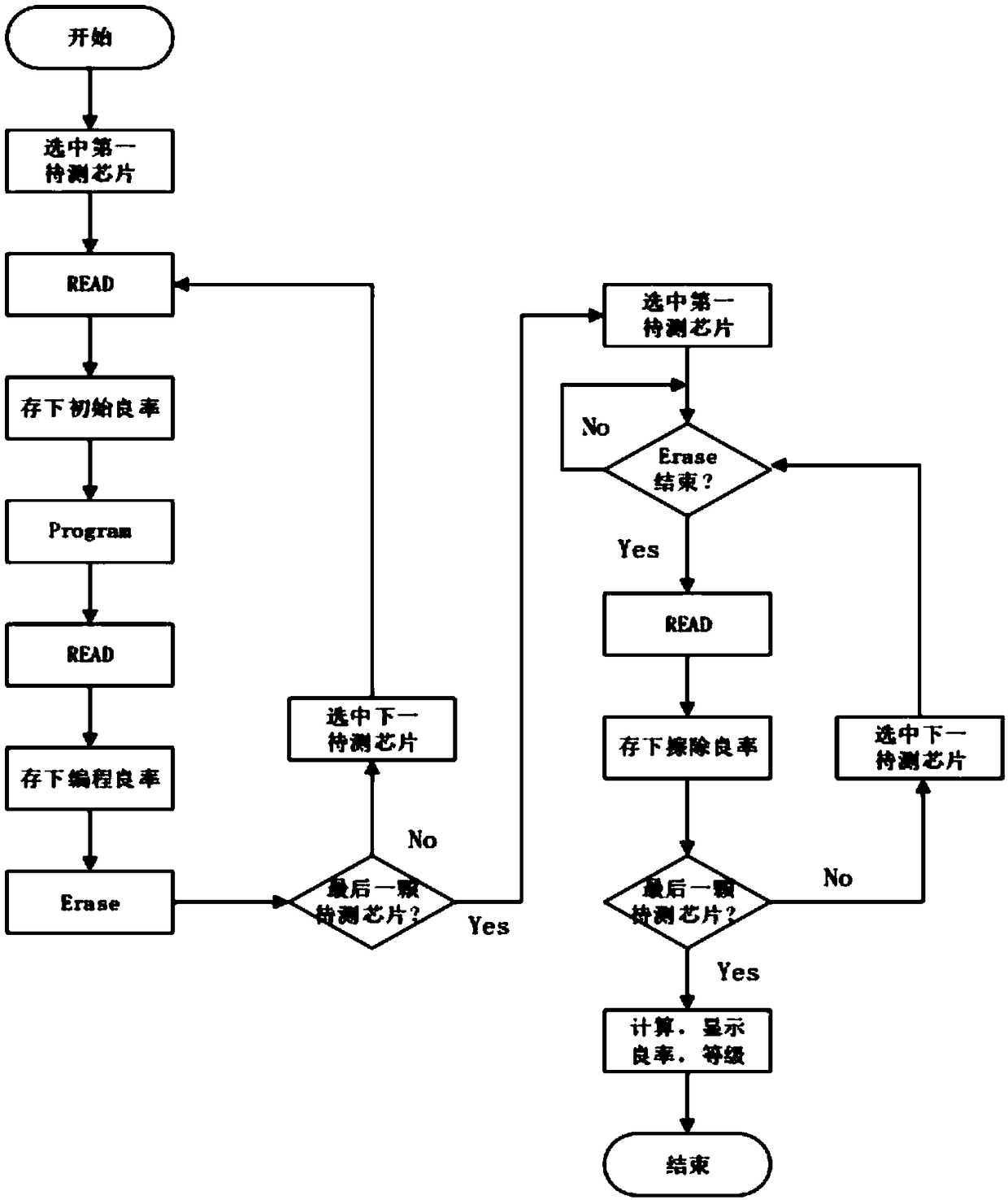
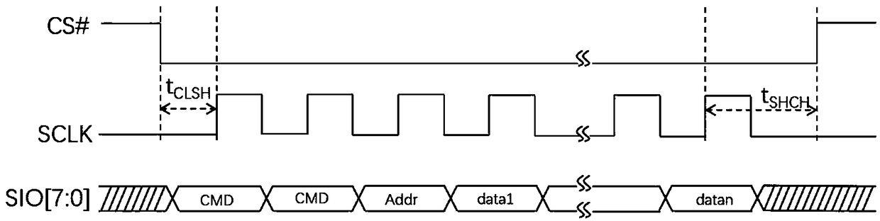
[0029] This embodiment provides an integrated circuit good product detection system, taking Octal SPI nor flash as an example, the system block diagram is as follows figure 1 As shown, it includes a control device, a display device, a decoder and several chips to be tested; the display device is connected to control transposition for displaying test results; the CS ports of several chips to be tested are connected to the control device through the decoder, and The clock interface sclk and data transmission interface io0~io7 of several chips to be tested adopt port multiplexing, that is, the clock interface sclk of each chip to be tested is connected to the same interface of the control device, and the data transmission interface of each chip to be tested io0~io7 respectively correspond to the same interface connected to the control device, such as figure 1 shown.

[...


PUM


Abstract

The invention belongs to the technical field of chip testing, and specifically provides a system and method for detecting non-defective products of integrated circuits. The system and method are usedfor realizing intelligent testing for multiple chips. The system comprises a control device, a display device, a decoder and a plurality of chips to be tested, wherein the display device is connectedwith the control device and used for displaying a detection result; chip selection signal ports of the plurality of chips to be tested are connected to the control device through the decoder, and a clock interface and data transmission interfaces of each chip to be tested are correspondingly connected to the identical interfaces of the control device. The system adopts a multiplexing technology ofthe clock interfaces and the data transmission interfaces of the chips to be tested, and the decoder matching the CS ends of the chips to be tested realizes the control of n io ports of the control device for 2n chips to be tested, thereby effectively overcoming a problem that a lot of IO ports are required in the testing for multiple chips; meanwhile, the test process is optimized, the test timeis greatly shortened, and the test efficiency is effectively improved; and high-efficiency and low-cost intelligent testing for the multiple chips is achieved.

Description

technical field [0001] The invention belongs to the technical field of chip testing, and relates to an intelligent, efficient, multi-chip, and less-channel testing system and method, in particular to a system and method for detecting good-quality integrated circuits. technical background [0002] Flash memory is used in computers and electronic equipment, automobiles, Internet of Things, drones, smart homes and other devices. These applications make flash most demanding higher transmission speed and lower power consumption; flash interface is extended from SPI To OPI (Octal SPI), by increasing the data transmission channel of serial nor flash, and supporting single, dual, quad or octal I / O interface; because Octal SPI is used to transmit data IO increased from 2 SPI to 8 , while the transmission data speed increases, the previous tests also need to occupy a large number of IO ports. [0003] Traditional chip testing requires manual control, especially the testing of SPI int...

Claims


Application Information

Patent Timeline
Patent Type & Authority Applications(China)
IPC IPC(8): G01R31/28
CPCG01R31/2851G01R31/2894
Inventor 高敏沈欣林媛潘泰松
Owner UNIV OF ELECTRONICS SCI & TECH OF CHINA
Why Eureka
Try Eureka