Array substrate and manufacturing method thereof

An array substrate and substrate technology, applied in semiconductor/solid-state device manufacturing, semiconductor devices, electrical components, etc., can solve problems such as display quality degradation, improve display quality, reduce overlapping areas, and reduce parasitic capacitance and resistance capacitance delayed effect

Active Publication Date: 2020-12-25
TCL CHINA STAR OPTOELECTRONICS TECH CO LTD
View PDF6 Cites 0 Cited by
  • Summary
  • Abstract
  • Description
  • Claims
  • Application Information

AI Technical Summary

Problems solved by technology

Therefore, when the above-mentioned thin film transistor is used as the transistor in the driving circuit, a considerable resistance-capacitance load (RC loading) will often be generated in signal transmission, resulting in a decrease in the display quality of the display.

Method used


Image

  • Array substrate and manufacturing method thereof
  • Array substrate and manufacturing method thereof
  • Array substrate and manufacturing method thereof

Examples


Embodiment Construction

[0041] The following descriptions of the various embodiments refer to the accompanying drawings to illustrate specific embodiments in which the present invention can be practiced. The directional terms mentioned in the present invention, such as "up", "down", "front", "back", "left", "right", "inside", "outside", "side", etc., are for reference only The orientation of the attached schema. Therefore, the directional terms used are used to illustrate and understand the present invention, but not to limit the present invention.

[0042] The invention is an array substrate and a method for manufacturing the array substrate. The array substrate is used for a display panel, and the display panel is a liquid crystal display panel (liquid crystal display, LCD) or an organic light emitting diode display panel (organic light emitting diode, OLED).

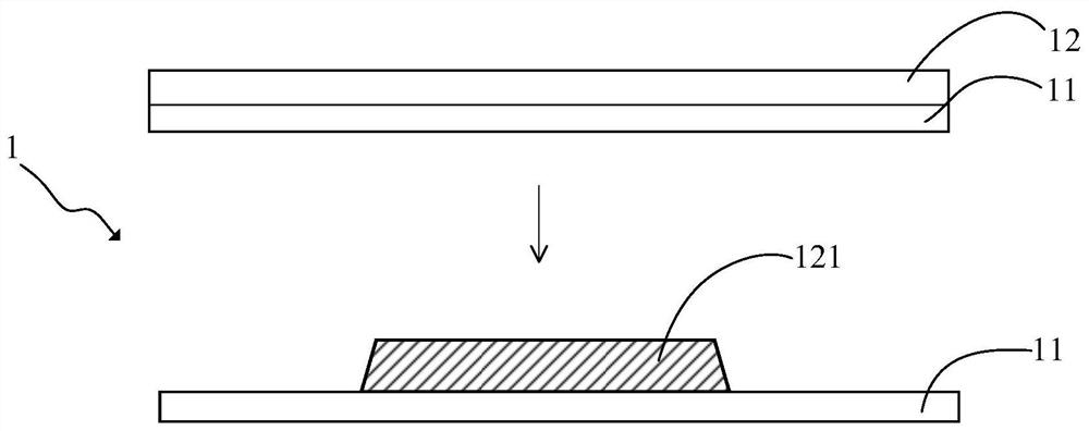
[0043] figure 1 It is a schematic diagram of a partial structure of an array substrate according to a preferred embodiment of the presen...


PUM


Abstract

An array substrate, used for a display panel. The array substrate comprises a substrate; a gate layer that is provided on the substrate and comprises a gate line; an organic photoresist layer that is coated on the gate layer and the substrate and provided with a groove corresponding to the gate line; a gate insulation layer provided on the organic photoresist layer; a metal oxide layer provided on the gate insulation layer; and a metal layer provided on the metal oxide layer, wherein the metal layer and the metal oxide layer define source and drain region circuits, a semiconductor region, and a pixel region by means of lithography and etching processes.

Description

【Technical field】 [0001] The present invention relates to the field of display technology, in particular to an array substrate for a display panel and a manufacturing method thereof. 【Background technique】 [0002] Liquid crystal display (LCD) and organic light emitting diode display (organic light emitting diode, OLED) are currently the most widely used display products in the market. Their production technology is very mature, the product yield rate is high, and the production cost is relatively low. High market acceptance. The thin film transistor (thin film transistor) display panel manufacturing industry has been developed for many years, and the production process of the product has been very refined and mature. [0003] As the resolution of LCD and OLED becomes higher and higher, the proportion of thin film transistors per unit area is also increasing. Also because the gate and the source of the TFT and between the gate and the drain partially overlap, the parasitic...

Claims


Application Information

Patent Timeline
Patent Type & Authority Patents(China)
IPC IPC(8): H01L27/12H01L21/77
CPCH01L27/1225H01L27/1259
Inventor 韦显旺
Owner TCL CHINA STAR OPTOELECTRONICS TECH CO LTD
Why Eureka
Try Eureka