Thin-film LED substrate for printing, printed thin-film LED device, and preparation method thereof
An LED device and printing technology are applied in the field of printing thin-film LED substrates, printing thin-film LED devices and their preparation fields, and can solve the problems of cumbersome preparation process, unfavorable LED functional layer ink printing, complex groove substrate structure, etc. , to achieve the effect of high design flexibility, simplified process complexity and high resolution
- Summary
- Abstract
- Description
- Claims
- Application Information
AI Technical Summary
Problems solved by technology
Method used
Image
Examples
preparation example Construction
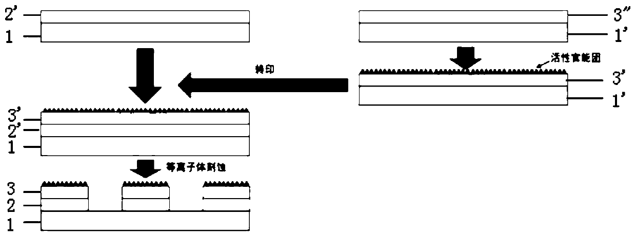
[0033] Correspondingly, combine figure 1 , as an implementation situation, an embodiment of the present invention provides a method for preparing a thin film LED substrate for printing, including the following steps:
[0034] S01. provide first substrate 1 and second substrate 1 ', deposit first graphene layer 2 ', second graphene layer 3 " on described first substrate 1, second substrate 1 ' respectively;
[0035] S02. After the second graphene layer 3 "is subjected to surface modification treatment, it is transferred to the surface of the first graphene layer 2' to form a composite graphene layer;
[0036] S03. According to the preset pixel array of the printed thin-film LED device, the composite graphene layer is patterned to form a patterned composite layer to obtain a thin-film LED substrate for printing.
[0037] Specifically, in the above step S01, the selection of the first substrate 1 and the second substrate 1' is not strictly selected. For details, refer to the abo...
Embodiment 1
[0072] A method for preparing a printed QLED device, comprising the following steps:
[0073] E11. Prepare QLED substrate for printing, including
[0074] E111. Depositing a first graphene layer on the first substrate by CVD, and depositing a second graphene layer on the second substrate;
[0075] E112. Utilizing concentrated sulfuric acid to carry out surface modification treatment on the second graphene layer, introducing active functional groups; transferring the second graphene layer after the surface modification treatment to the surface of the first graphene layer to form composite graphite vinyl layer;
[0076] E113. Plasma etching the composite graphene layer to form a patterned composite layer to obtain a QLED substrate for printing.
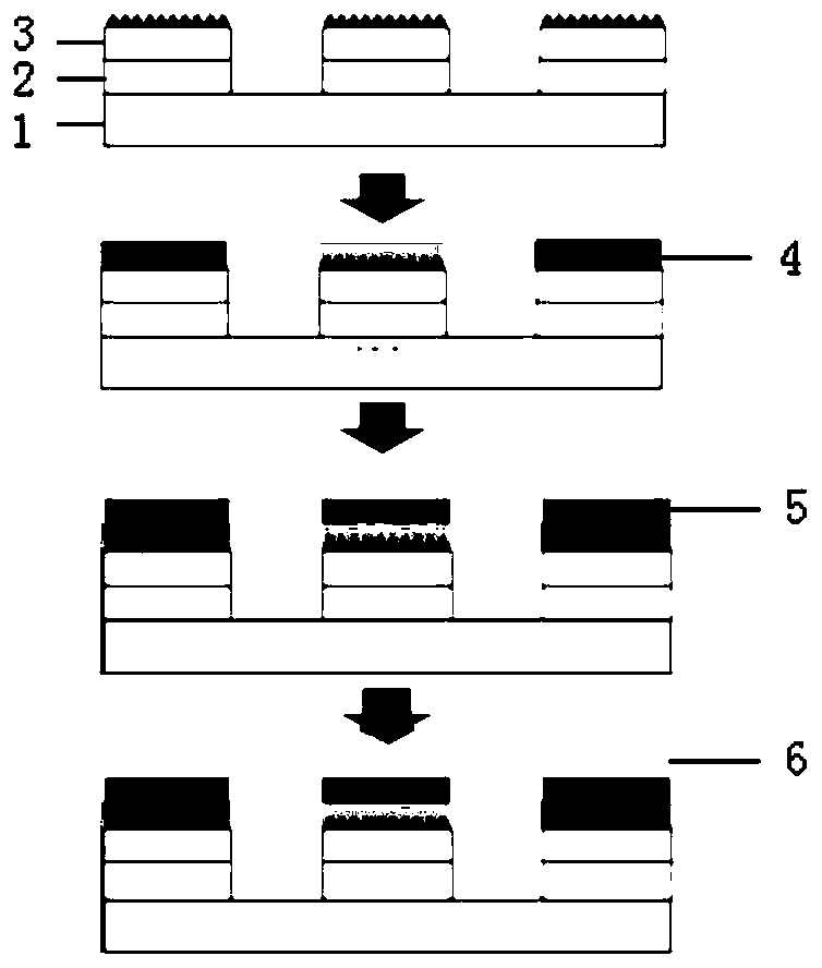
[0077] E12. Printing a CdSe / ZnS quantum dot light-emitting layer and a ZnO electron transport layer sequentially on the patterned composite layer in the QLED substrate for printing, and depositing an Al cathode to obtain a printed QLE...
Embodiment 2
[0079] A method for preparing a printed OLED device, comprising the following steps:
[0080] E21. Preparation of OLED substrate for printing, including
[0081] E211. Depositing a first graphene layer on the first substrate by CVD method, and depositing a second graphene layer on the second substrate;
[0082] E212. Using concentrated sulfuric acid to carry out surface modification treatment on the second graphene layer to introduce active functional groups; transfer the surface modification treatment of the second graphene layer to the surface of the first graphene layer to form composite graphite vinyl layer;
[0083] E213. Plasma etching the composite graphene layer to form a patterned composite layer to obtain an OLED substrate for printing.
[0084] E22. Printing the light-emitting layer / electron transport layer sequentially in the groove area of the OLED substrate for printing, and depositing the Al cathode to obtain a printed OLED device.
PUM
| Property | Measurement | Unit |
|---|---|---|
| electron work function | aaaaa | aaaaa |
| thickness | aaaaa | aaaaa |
| thickness | aaaaa | aaaaa |
Abstract
Description
Claims
Application Information

