

Preparation method of semiconductor probe tip sample for detection of three-dimensional atom probe
An atomic probe and semiconductor technology, applied in the field of micro-nano-scale material sample preparation, can solve problems such as data distortion and large differences in element evaporation fields, so as to improve efficiency, reduce sampling steps, and reduce the possibility of needle tip sample breakage Effect
- Summary
- Abstract
- Description
- Claims
- Application Information
AI Technical Summary
Problems solved by technology
Method used
Image


Examples
Embodiment Construction
[0041] The present invention will be described in further detail below in conjunction with the accompanying drawings.
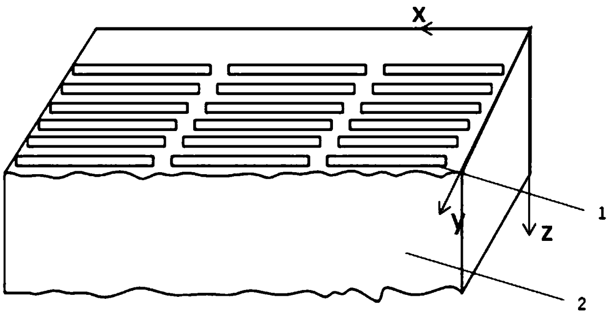
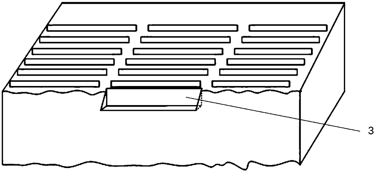
[0042] By using the fin structure sample processing technology in the cross-cut fin field effect transistor of the present invention, the fin structure of the fin field effect transistor can be prepared for three-dimensional atom probe tip samples. This method is different from the traditional method of vertically placing the entire fin structure on a needle tip, but adopts a segmented method, cross-cutting the fin structure in the semiconductor device, and placing the fin structure in the semiconductor device perpendicular to the growth direction. Use the focused ion beam to cut into a small section, that is, only a small section of the fin structure is included in each 3D atom probe tip sample, and then cut multiple needle tips, and after collecting the 3D atom probe data for all the tip, that is Can be combined to form a complete fin structure.
[0043] T...
PUM
| Property | Measurement | Unit |
|---|---|---|
| Thickness | aaaaa | aaaaa |
| Diameter | aaaaa | aaaaa |
Abstract
Description
Claims
Application Information