Method for extracting scattering parameters of electron beam exposure

A technology of electron beam exposure and scattering parameters, applied in the field of electron beam exposure, can solve the problems of complicated operation and difficulty in ensuring accuracy, and achieve the effect of reducing errors, accurate parameter extraction and simple and easy operation.

Inactive Publication Date: 2019-02-12
吴辉
View PDF0 Cites 0 Cited by
  • Summary
  • Abstract
  • Description
  • Claims
  • Application Information

AI Technical Summary

Problems solved by technology

[0006] In order to solve the problem of cumbersome operation and difficulty in ensuring accuracy in the existing method for extracting scattering parameters of electron beam exposure, the present invention provides a method for extracting scattering parameters of electron beam exposure, which does not require a large number of cumbersome measurements and data preprocessing and data processing. Fitting, so there is no measurement error, and reduces the error caused by mathematical processing, making parameter extraction accurate and easy

Method used


Image

  • Method for extracting scattering parameters of electron beam exposure
  • Method for extracting scattering parameters of electron beam exposure
  • Method for extracting scattering parameters of electron beam exposure

Examples


Embodiment

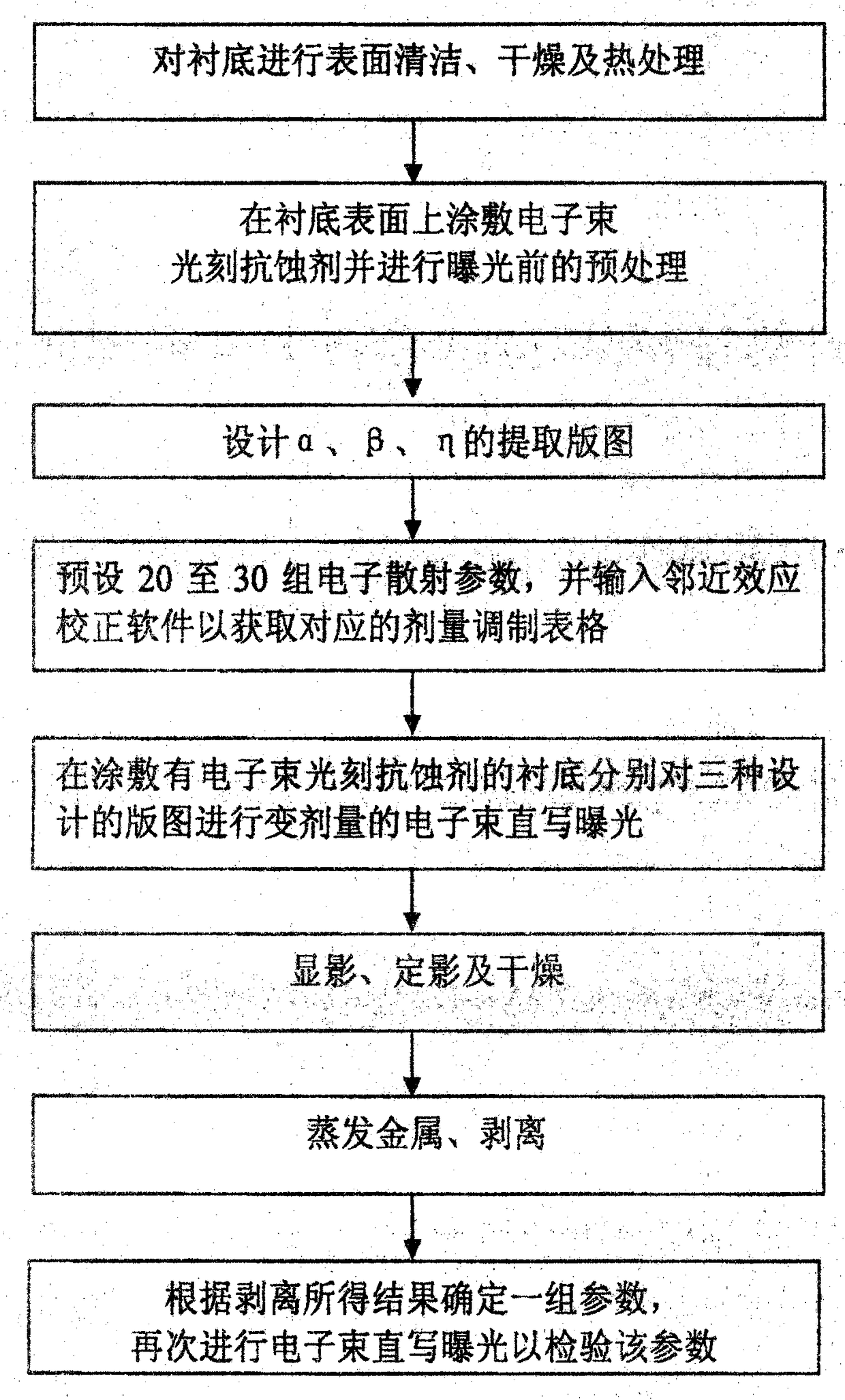
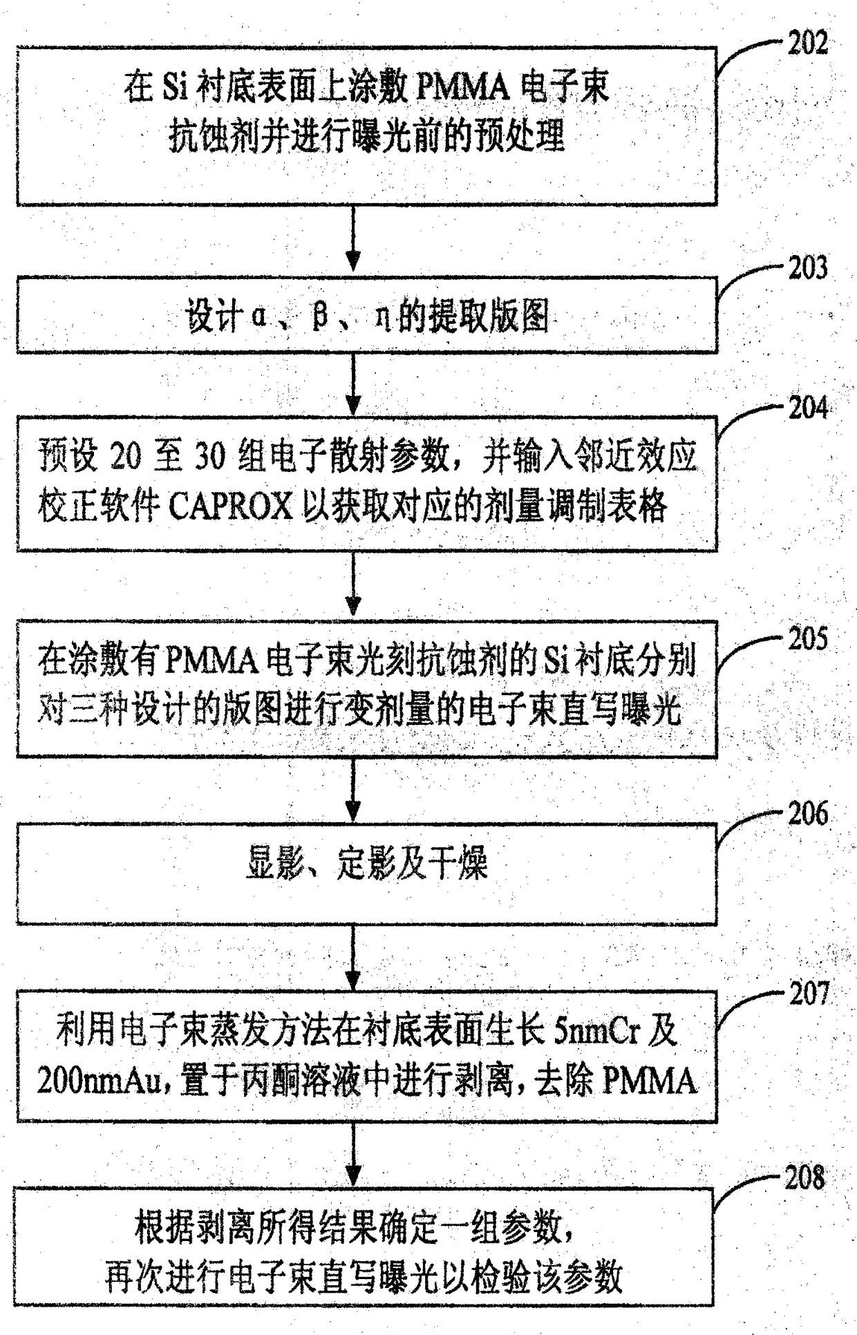
[0050] In this embodiment, a polymethyl methacrylate PMMA positive electron resist is used as an example, and the method for extracting electron beam exposure scattering parameters provided by the present invention is further described in conjunction with the accompanying drawings.

[0051] Step 201: Perform surface cleaning and heat treatment on the two-inch silicon wafer substrate;

[0052] In this step, a batch (20 pieces) of new silicon wafers are rinsed with deionized water, and then placed in a special container filled with concentrated sulfuric acid and heated at about 300°C for 40 minutes. After cooling, take out the silicon wafers and use deionized water. Rinse it with water, place it in an oven, and bake at 180°C for 2 hours until the water vapor completely evaporates.

[0053] Step 202: Spin-coating a PMMA electron beam photolithography resist layer on the surface of the Si substrate, and conduct a pre-baking treatment on a hot plate at 180°C for 2 minutes to allow the org...


PUM

PropertyMeasurementUnit
thicknessaaaaaaaaaa

Abstract

The invention relates to a method for extracting scattering parameters of electron beam exposure, aiming at solving the problems that the existing method for extracting the scattering parameters of the electron beam exposure is complicated in operation and difficult in guarantee of accuracy. The invention provides the method for extracting the scattering parameters of the electron beam exposure; the method comprises the steps of deigning proper extraction domains of a front scattering parameter alpha, a back scattering parameter beta and a deposition energy ratio eta of back scattering to front scattering according to the characteristics of an electron beam resist and a substrate structure which are about to be subjected to parameter extraction; then, separately performing variable dose electron beam direct writing exposure on the three designed extraction domains on the electron beam resist and the substrate structure which are to be tested; finally, determining the group of suitablescattering parameters according to the pattern structure characteristics of the multiple groups of different parameters after exposure, development and stripping. After the method is adopted, a greatdeal of tedious measurement does not need to be performed, so that measurement error is avoided, and the error caused by the mathematical processing is reduced; therefore, the method enables parameterextraction to be accurate, simple and east to implement.

Description

Technical field [0001] The invention relates to the technical field of electron beam exposure, in particular to a method for extracting scattering parameters of electron beam exposure. Background technique [0002] Electron beam exposure technology (including electron beam direct writing exposure and projection exposure) is an important means of modern micro-nano processing, and it is also a strong candidate for the next generation of lithography technology. Since the wavelength of the electron beam is extremely short (when the accelerating voltage is 15-20kv, the wavelength is about 0.1-0.07 angstroms), it will not be limited by the diffraction effect like optical lithography and can achieve higher resolution. However, the diffusion of the exposure range caused by the scattering of incident electrons in the resist layer and the substrate restricts the improvement of its resolution and affects the imaging quality. For example, the contour of the graphic expands to the adjacent a...

Claims


Application Information

Patent Timeline
Patent Type & Authority Applications(China)
IPC IPC(8): G03F7/20
CPCG03F7/2061G03F7/70491
Inventor 吴辉
Owner 吴辉
Why Eureka
Try Eureka