Memory formation method

A memory and semiconductor technology, which is used in the manufacture of electrical solid-state devices, semiconductor devices, and semiconductor/solid-state devices. possibility, strain reduction, effect of grain size reduction

Active Publication Date: 2019-02-12
YANGTZE MEMORY TECH CO LTD
View PDF4 Cites 4 Cited by
  • Summary
  • Abstract
  • Description
  • Claims
  • Application Information

AI Technical Summary

Problems solved by technology

The polysilicon layer has less strain after subsequent high-temperature annealing, but usually there is a gap with the inner wall surface of the gate line spacer, which cannot be completely attached to the surface of the gate line spacer, and voids are prone to appear inside, which affects the final formed memory performance; the amorphous semiconductor material layer can fill the gate line spacer, and...

Method used


Image

  • Memory formation method
  • Memory formation method
  • Memory formation method

Examples


Embodiment Construction

[0022] A memory and its forming method proposed by the present invention will be described in detail below with reference to the drawings and specific embodiments.

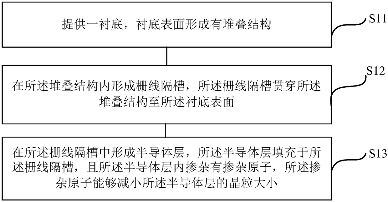
[0023] see figure 1 , is a flow chart of the method for forming the memory in a specific implementation manner. The forming method of the memory includes the following steps: S11: Provide a substrate, and a stack structure is formed on the surface of the substrate. S12: Forming a gate line spacer in the stack structure, the gate line spacer penetrating through the stack structure to the surface of the substrate. S13: forming a semiconductor layer in the gate line spacer, the semiconductor layer is filled in the gate line spacer, and the semiconductor layer is doped with dopant atoms, and the dopant atoms can reduce the The grain size of the semiconductor layer.

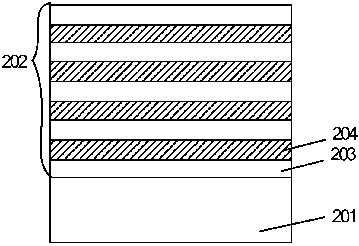
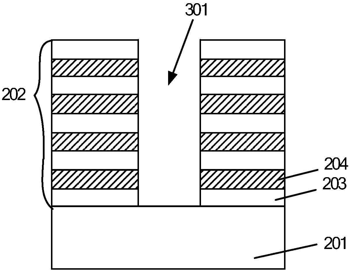
[0024] see Figure 2 to Figure 6 , is a schematic structural diagram of a memory forming process according to a specific embodiment of the present in...


PUM


Abstract

The invention relates to a memory formation method. The memory formation method comprises the following steps: providing a substrate, wherein a stacking structure is formed on the surface of the substrate; forming a grid line spacer groove in the stacking structure, wherein the grid line spacer groove penetrates through the stacking structure and then extends to the surface of the substrate; and forming a semiconductor layer in the grid line spacer groove, wherein the grid line spacer groove is filled with the semiconductor layer, the inside of the semiconductor layer is doped with doping atoms, and the grain size of the semiconductor layer can be reduced by the doping atoms. The grains of the semiconductor layers formed by the method are small, and the performance of a memory can be improved.

Description

technical field [0001] The invention relates to the technical field of semiconductors, in particular to a method for forming a memory. Background technique [0002] In recent years, the development of flash memory (Flash Memory) is particularly rapid. The main feature of flash memory is that it can keep stored information for a long time without power on, and has the advantages of high integration, fast access speed, easy erasing and rewriting, etc. Has been widely used. In order to further increase the bit density (Bit Density) of the flash memory while reducing the bit cost (Bit Cost), three-dimensional flash memory (3D NAND) technology has been developed rapidly. [0003] In the process of forming a 3D NAND memory, it is necessary to form a stacked structure consisting of a sacrificial layer and an insulating layer on the surface of the substrate, then etch the stacked structure to form a gate line spacer, and then fill the gate line spacer with a semiconductor layer ....

Claims


Application Information

Patent Timeline
IPC IPC(8): H01L21/02H01L21/324H01L27/11524H01L27/11551H01L27/1157H01L27/11578H01L29/167
CPCH01L29/167H01L21/02532H01L21/02592H01L21/0262H01L21/02667H01L21/324H10B41/20H10B41/35H10B43/20H10B43/35
Inventor 王秉国宋海李磊
Owner YANGTZE MEMORY TECH CO LTD
Why Eureka
Try Eureka