Method for rapidly detecting silicon crystal defects on semiconductor wafer substrate

A detection method and technology of silicon crystal, applied in semiconductor/solid state device testing/measurement, electrical components, circuits, etc., can solve problems such as influence, difficulty in obtaining repeatable scribing results, achieve accurate repeatability, and avoid artificial defect artifacts , the effect of good etching effect

Inactive Publication Date: 2019-02-19
胜科纳米(苏州)股份有限公司
View PDF4 Cites 2 Cited by
  • Summary
  • Abstract
  • Description
  • Claims
  • Application Information

AI Technical Summary

Problems solved by technology

[0003] However, in actual production, the current traditional method is to directly etch without removing the upper layer of the substrate material and polysilicon, but it is difficult to obtain a repeatable scribing result in this way, and some New defects lead to subsequent false defects, which in turn affects the judgment of the cause of the defect

Method used


Image

  • Method for rapidly detecting silicon crystal defects on semiconductor wafer substrate

Examples


Embodiment Construction

[0017] In order to make the above objects, features and advantages of the present invention more comprehensible, specific implementations of the present invention will be described in detail below in conjunction with the accompanying drawings. It should be noted that all the drawings of the present invention are in simplified form and use inaccurate scales, and are only used to facilitate and clearly assist the purpose of illustrating the embodiments of the present invention.

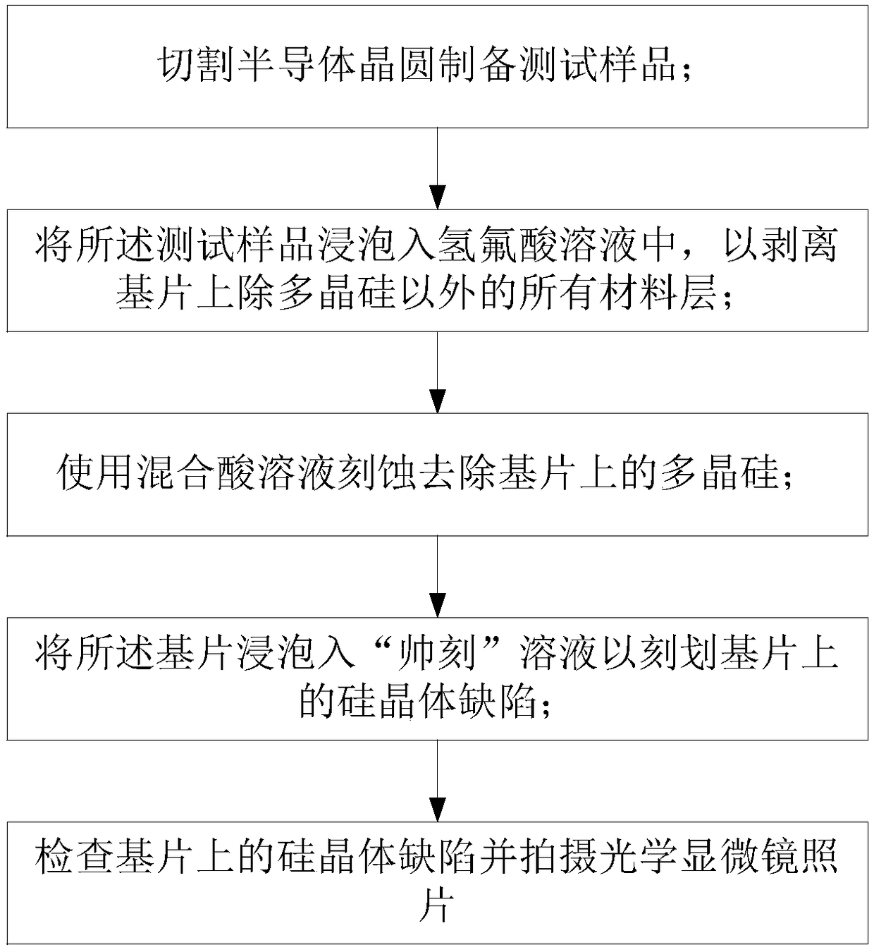
[0018] Such as figure 1 As shown, the present invention provides a kind of rapid detection method of silicon crystal defect on semiconductor wafer substrate, comprising:

[0019] Cut the semiconductor wafer to prepare the required test samples. Generally, the length and width of the test samples are selected as 2x2 cm in size;

[0020] The test sample was immersed in a hydrofluoric acid solution to peel off all material layers in the test sample except the substrate and the polysilicon layer. Wherein,...


PUM


Abstract

The invention discloses a method for rapidly detecting silicon crystal defects on a semiconductor wafer substrate. The method includes the steps: cutting a semiconductor wafer to prepare a test sample; soaking the test sample into hydrofluoric acid solution to strip all material layers except for polycrystalline silicon on the substrate; etching and removing the polycrystalline silicon on the substrate by mixed acid solution; soaking the substrate into 'smart etching' solution to scratch the silicon crystal defects on the substrate; checking the silicon crystal defects on the substrate and taking optical microphotographs or scanning electron microphotographs. A complete test sample treatment method is built, particularly, before the silicon crystal defects on the substrate are scratched bythe 'smart etching' solution, all materials on an upper layer of the silicon substrate are thoroughly stripped, so that the substrate is fully naked and then subjected to 'smart etching', good etching effects are achieved, artificial defect illusion caused by incomplete stripping of the materials on the upper layer of the substrate is avoided, and accurate and good-repeatability scratching results are acquired.

Description

technical field [0001] The invention relates to the field of semiconductor manufacturing, in particular to a rapid detection method for silicon crystal defects on a semiconductor wafer substrate. Background technique [0002] In the manufacture of semiconductor wafer discs, silicon crystal defects on the substrate directly affect the yield of wafers. Therefore, in failure analysis, failure analysis engineers need to discover silicon crystal defects on the substrate and find out the causes of it, so as to improve the production process and increase the yield. [0003] However, in actual production, the current traditional method is to directly etch without removing the upper layer of the substrate material and polysilicon, but it is difficult to obtain a repeatable scribing result in this way, and some New defects will lead to subsequent false defects, which will affect the judgment of the cause of defects. Contents of the invention [0004] The invention provides a rapid...

Claims


Application Information

Patent Timeline
Patent Type & Authority Applications(China)
IPC IPC(8): H01L21/66
CPCH01L22/12
Inventor 华佑南李兵海李晓旻
Owner 胜科纳米(苏州)股份有限公司
Why Eureka
Try Eureka