Degradable self-supported thin-film transistor device and production method thereof

A self-supporting thin film and transistor technology, which is applied in semiconductor/solid-state device manufacturing, transistors, semiconductor devices, etc., can solve environmental pollution and other problems, and achieve the effects of simple preparation process, good channel regulation performance, and simplified material structure

Inactive Publication Date: 2019-02-19
NANCHANG INST OF TECH
View PDF9 Cites 6 Cited by
  • Summary
  • Abstract
  • Description
  • Claims
  • Application Information

AI Technical Summary

Problems solved by technology

[0003] With the rapid development of electronic preparation technology, damaged or obsolete electronic devices are abandoned every moment, which will lead to serious environmental pollution

Method used


Image

  • Degradable self-supported thin-film transistor device and production method thereof
  • Degradable self-supported thin-film transistor device and production method thereof

Examples


Embodiment Construction

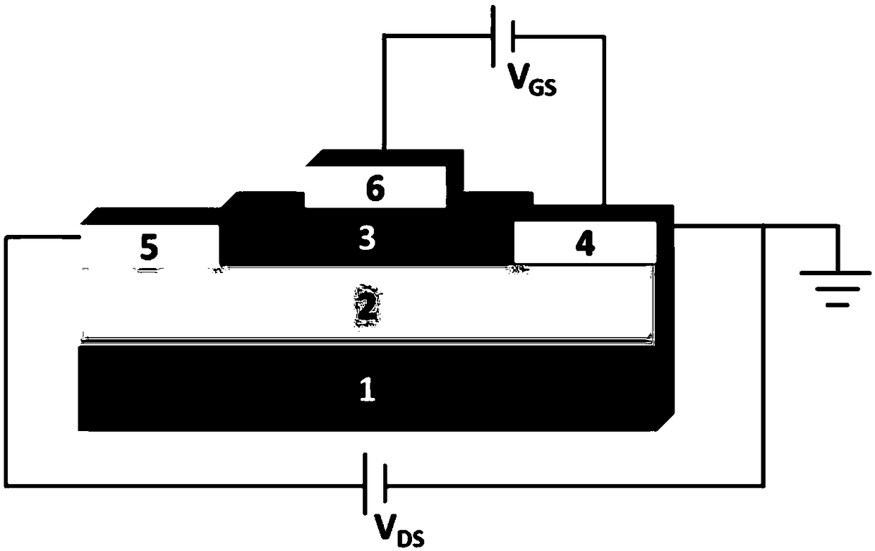
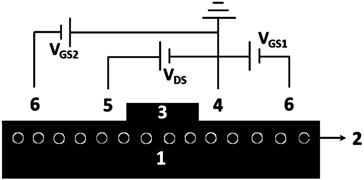
[0025] Such as figure 2 As shown, the present invention works and implements like this, a degradable self-supporting thin film transistor device mainly includes a self-supporting dielectric layer 1, a semiconductor active layer 3, a source electrode 4, a drain electrode 5 and a gate electrode 6 ; It is characterized in that: the degradable self-supporting thin film transistor device adopts the natural high molecular polymer film with ion-conducting properties of movable ions 2 in the dielectric layer as the self-supporting dielectric layer 1, on the self-supporting dielectric layer 1 Then deposit the semiconductor active layer 3 and the coplanar source electrode 4 , drain electrode 5 and gate electrode 6 in sequence, wherein the semiconductor active layer 3 is arranged between the source electrode 4 and the drain electrode 5 .

[0026] A method for preparing a degradable self-supporting thin film transistor device according to the present invention is characterized in that th...


PUM


Abstract

The invention discloses a degradable self-supported thin-film transistor device, mainly comprising a self-supported dielectric layer, a semiconductor active layer, a source electrode, a drain electrode and a gate electrode, and characterized in that natural macromolecular polymer film having ionic conductivity is used herein as the self-supported dielectric layer, and the semiconductor active layer and the coplanar source electrode, drain electrode and gate electrode are deposited on the self-supported dielectric layer in sequence, wherein the semiconductor active layer is arranged between thesource electrode and the drain electrode. The degradable self-supported thin-film transistor device has the advantages that the dielectric layer having supporting performance is used herein, extra substrates are not required, and the material structure of the degradable self-supported thin-film transistor device is simplified; the natural macromolecular polymer film has low cost and has good stability under room-temperature conventional environments; by controlling composition and structure of the film herein, it is possible to adjust the degradation rate of the film in a special environment,and therefore, the thin-film transistor device with controllable degradation rate is achieved.

Description

technical field [0001] The invention relates to the technical field of semiconductor devices, in particular to a degradable self-supporting thin film transistor device and a preparation method thereof. Background technique [0002] At present, various electronic devices are usually made of non-degradable, very stable, and possibly even toxic (such as gallium arsenide) substrate materials and electronic components in order to perform their functions stably. Thin film transistors are the most basic electronic components, and have been widely used in random access memory, flat panel display, photoelectric sensor and other fields. [0003] With the rapid development of electronic preparation technology, damaged or obsolete electronic devices are abandoned every moment, which will lead to serious environmental pollution. On the other hand, with the development and application of implantable medical devices, thin film transistor devices that are biocompatible and can degrade and ...

Claims


Application Information

Patent Timeline
Patent Type & Authority Applications(China)
IPC IPC(8): H01L29/786H01L21/34
CPCH01L29/66969H01L29/78603H01L29/78693
Inventor 刘宁刘宇胡军平张晓航
Owner NANCHANG INST OF TECH
Why Eureka
Try Eureka