Back polishing technology for low-cost solar battery

A solar cell and backside polishing technology, which is applied in the direction of circuits, photovoltaic power generation, electrical components, etc., can solve the problems such as the bad influence of the back reflection of the incident light on the battery, achieve a significant passivation effect, increase the output current, and reduce the effect of transmission loss

Active Publication Date: 2019-02-19
RENESOLA JIANGSU LTD
View PDF5 Cites 9 Cited by
  • Summary
  • Abstract
  • Description
  • Claims
  • Application Information

AI Technical Summary

Problems solved by technology

[0002] Solar energy has unique characteristics such as cleanness and regeneration. Therefore, solar photovoltaic utilization has become the fastest-growing research field in recent years. At present, people's research on solar cells is mainly focused on improving the conversion efficiency of batteries and reducing costs. People have developed a variety of battery structures, such as electrodes made by SE technology, buried gate electrodes, and passivated back of the battery. Changes in these structures will increase the battery manufacturing process steps and increase the cost of battery manufacturing. In order to reduce the cost of the battery , the use of ultra-thin silicon wafers to prepare high-efficiency solar cells has become a research direction; however, as the thickness of the cells decreases to 180um, the loss of long-wave light absorption by the cells becomes more serious due to the thickness of the cells; therefore, it is necessary to Optimize the structure of the back surface of the battery to improve the reflectivity of long-wave light on the back surface of the battery
[0003] In order to improve the reflectance of the back surface of the battery to the incident long-wave light, people use a dielectric film to improve the reflection of the incident light, which can effectively improve the reflection of the incident light on the back surface of the battery. However, due to the conventional texture The suede on the back surface of the process has a light-trapping structure, so it will have a negative impact on the back reflection of the incident light of the battery

Method used


Image

  • Back polishing technology for low-cost solar battery

Examples


Embodiment 1

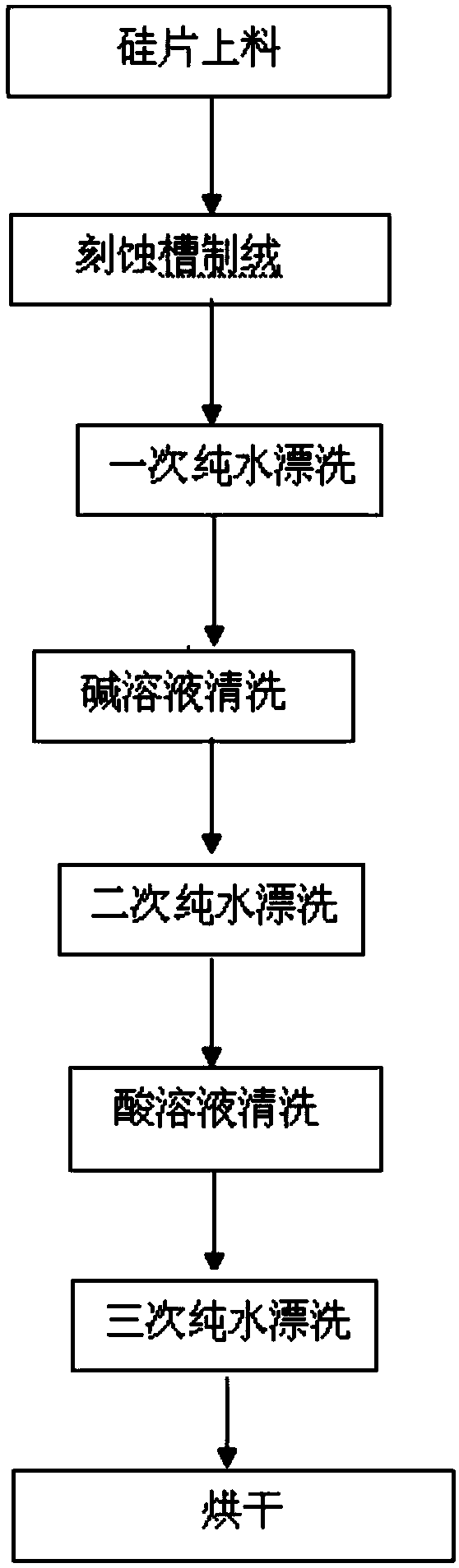
[0034] A kind of low-cost solar cell back polishing process that this embodiment provides, flow process is as follows figure 1 As shown, it includes the following process: silicon wafer feeding - cleaning silicon wafer surface oil stain - silicon wafer surface texturing and polishing - pure water rinsing - alkali cleaning - second pure water rinsing - pickling - three pure water rinsing - drying ,in:

[0035] T1: Silicon wafer loading, polycrystalline diamond wire cut silicon wafer is selected, and the thickness of the silicon wafer is 180um;

[0036] T2: Etching groove to make texture, place the silicon wafer in the etching groove to control the reaction speed of the upper and lower surfaces of the silicon wafer, so that the reflectance of the textured side of the silicon wafer is 21%-23%, and the non-textured surface on the back of the silicon wafer is polished, the reflectivity Control at 40%-55%;

[0037] The making of the texturing tank solution is specifically: the tex...

Embodiment 2

[0050] A kind of low-cost solar cell back polishing process that this embodiment provides, flow process is as follows figure 1 As shown, it includes the following process: silicon wafer feeding - cleaning silicon wafer surface oil stain - silicon wafer surface texturing and polishing - pure water rinsing - alkali cleaning - second pure water rinsing - pickling - three pure water rinsing - drying ,in:

[0051] T1: Silicon wafer loading, polycrystalline diamond wire cut silicon wafer is selected, and the thickness of the silicon wafer is 180um;

[0052] T2: Etching groove to make texture, place the silicon wafer in the etching groove to control the reaction speed of the upper and lower surfaces of the silicon wafer, so that the reflectivity of the textured side of the silicon wafer is 21%, and the non-textured surface of the silicon wafer is polished, and the reflectivity is controlled at 40%%;

[0053] The making of the texturing tank solution is specifically: the texturing t...

Embodiment 3

[0066] A kind of low-cost solar cell back polishing process that this embodiment provides, flow process is as follows figure 1 As shown, it includes the following process: silicon wafer feeding - cleaning silicon wafer surface oil stain - silicon wafer surface texturing and polishing - pure water rinsing - alkali cleaning - second pure water rinsing - pickling - three pure water rinsing - drying ,in:

[0067] T1: Silicon wafer loading, polycrystalline diamond wire cut silicon wafer is selected, and the thickness of the silicon wafer is 180um;

[0068] T2: Etching groove to make texture, place the silicon wafer in the etching groove to control the reaction speed of the upper and lower surfaces of the silicon wafer, so that the reflectance of the textured side of the silicon wafer is 23%, and the non-textured back of the silicon wafer is polished, and the reflectance is controlled at 55 %;

[0069] The making of the texturing tank solution is specifically: the texturing tank s...


PUM

PropertyMeasurementUnit
volumeaaaaaaaaaa

Abstract

The invention discloses a back polishing technology for a low-cost solar battery. The technology comprises the following process: loading a silicon wafer, washing greasy dirt on the surface of the silicon wafer, texturing and polishing the surface of the silicon wafer, rinsing by pure water, alkali-washing, secondary-rinsing by the pure water, acid-picking, third-rinsing by the pure water, and blow-drying. The technology is simple and easy to operate, and good in back polishing effect. The silicon wafer after polishing has good optical gain and the remarkable passivation effect.

Description

technical field [0001] The invention relates to the technical field of production and manufacture of crystalline silicon solar cells, in particular to a low-cost solar cell back polishing process. Background technique [0002] Solar energy has unique characteristics such as cleanness and regeneration. Therefore, solar photovoltaic utilization has become the fastest-growing research field in recent years. At present, people's research on solar cells is mainly focused on improving the conversion efficiency of batteries and reducing costs. People have developed a variety of battery structures, such as electrodes made by SE technology, buried gate electrodes, and passivated back of the battery. Changes in these structures will increase the battery manufacturing process steps and increase the cost of battery manufacturing. In order to reduce the cost of the battery , the use of ultra-thin silicon wafers to prepare high-efficiency solar cells has become a research direction; howev...

Claims


Application Information

Patent Timeline
Patent Type & Authority Applications(China)
IPC IPC(8): H01L31/18
CPCH01L31/1804H01L31/1868Y02E10/547Y02P70/50
Inventor 马建峰张敬敬丁振华李景龙宋令枝郭敏梅金丽葛祖荣
Owner RENESOLA JIANGSU LTD
Why Eureka
Try Eureka