Geomagnetic sensing device and manufacturing method thereof

A technology of a geomagnetic sensor and a manufacturing method, which is applied in the direction of measuring the geometric arrangement of magnetic sensing elements, electric solid-state devices, semiconductor devices, etc., can solve the problems of cumbersome manufacturing process, unfavorable signal transmission, and low integration density, so as to improve accuracy and increase Integration level, the effect of reducing package pins

Pending Publication Date: 2019-02-22
HANGZHOU SILAN INTEGRATED CIRCUIT +1
View PDF0 Cites 4 Cited by
  • Summary
  • Abstract
  • Description
  • Claims
  • Application Information

AI Technical Summary

Problems solved by technology

The inter-module interconnection of SIP is very long and the integration density is low, which is not conducive to signal transmission, and the manufacturing process is cumbersome and not conducive to integration.

Method used


Image

  • Geomagnetic sensing device and manufacturing method thereof
  • Geomagnetic sensing device and manufacturing method thereof
  • Geomagnetic sensing device and manufacturing method thereof

Examples


Embodiment Construction

[0048] Hereinafter, the present invention will be described in more detail with reference to the accompanying drawings. In the various figures, identical elements are indicated with similar reference numerals. For the sake of clarity, various parts in the drawings have not been drawn to scale. Also, some well-known parts may not be shown.

[0049] In the following, many specific details of the present invention are described, such as device structures, materials, dimensions, processing techniques and techniques, for a clearer understanding of the present invention. However, the invention may be practiced without these specific details, as will be understood by those skilled in the art.

[0050] The invention can be embodied in various forms, some examples of which are described below.

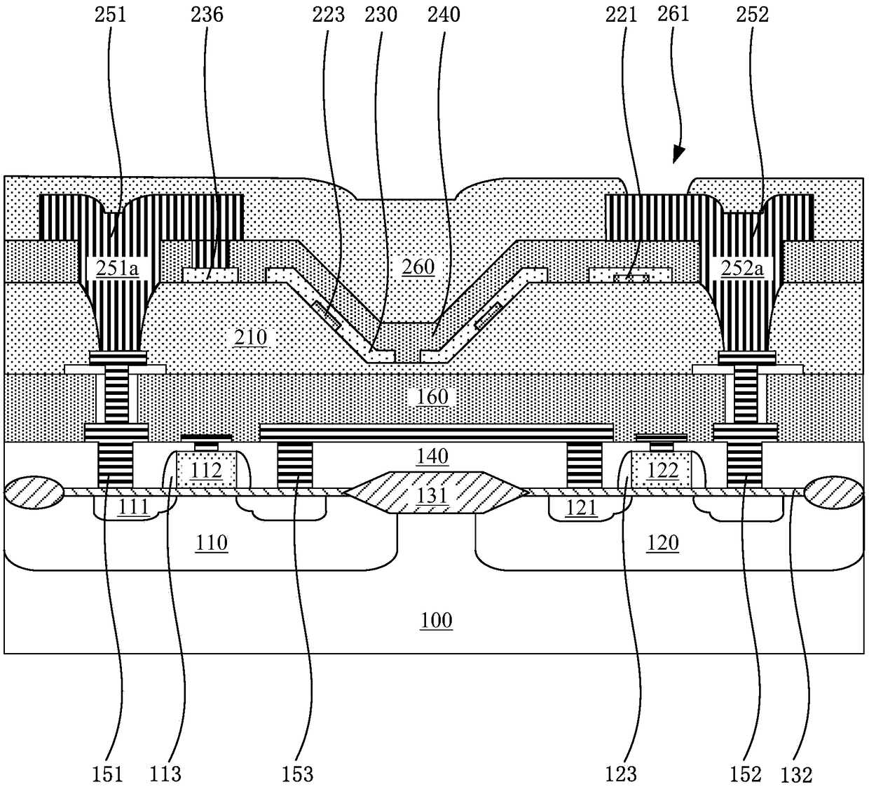
[0051] figure 1 A schematic cross-sectional view of a geomagnetic sensor device according to an embodiment of the present invention is shown.

[0052] Such as figure 1 As shown, the geoma...


PUM

PropertyMeasurementUnit
thicknessaaaaaaaaaa
thicknessaaaaaaaaaa

Abstract

The invention discloses a geomagnetic sensing device and a manufacturing method thereof. The geomagnetic sensing device comprises a CMOS circuit and a sensor located on the CMOS circuit; the CMOS circuit is connected with the sensor and used for driving the sensor and processing a detection signal generated by the sensor; and the sensor comprises a structure layer, magnetic resistance strips, short circuit electrodes, metal wires, a first conducting layer and a second conducting layer, wherein the magnetic resistance strips, the short circuit electrodes and the metal wires are sequentially formed on the structure layer, the first conducting layer and the second conducting layer are located over the structure layer, the first conducting layer is connected with the CMOS circuit and the metalwires, and the second conducting layer is connected with the CMOS circuit and an external circuit. By forming the sensor on the CMOS circuit and achieving electrical connection of the CMOS circuit and the sensor through the first conducting layer and the second conducting layer, the functions that the CMOS circuit drives the sensor and processes the detection signal generated by the sensor are achieved, and the purpose of integrating the CMOS circuit with the sensor is achieved.

Description

technical field [0001] The present disclosure relates to the technical field of semiconductors, and more particularly, to a geomagnetic sensor device and a manufacturing method thereof. Background technique [0002] Micro-Electro-Mechanical System (MEMS) and integrated circuit (integrated circuit, IC) are currently the two most important development areas of the semiconductor industry. Driven by the rapid development of global science and technology, the integration of MEMS and IC has become an inevitable trend. There are three integration methods: monolithic integration, semi-hybrid (bonding) integration and hybrid integration. Monolithic integration means that the MEMS structure and CMOS are fabricated on one chip. Hybrid integration is to manufacture MEMS and IC on different dies, and then package them in a package, and connect the bare MEMS chip with bumps to the IC chip in the form of flip-chip welding or wire bonding to form a SIP. . Semi-hybrid is the use of three...

Claims


Application Information

Patent Timeline
Patent Type & Authority Applications(China)
IPC IPC(8): B81B7/00B81C1/00G01R33/00G01R33/09
CPCB81B7/0006B81B7/0009B81B2201/0292B81C1/00063B81C1/0023B81C1/00301G01R33/0005G01R33/09
Inventor 孙伟刘琛高周妙罗燕飞闻永祥
Owner HANGZHOU SILAN INTEGRATED CIRCUIT
Why Eureka
Try Eureka