Light emitting diode and preparation method thereof, and application thereof

A technology of light-emitting diodes and light-emitting layers, which is applied in the manufacture of semiconductor/solid-state devices, electrical components, and electric solid-state devices. Effects of light extraction efficiency, increase in electrical stability and mechanical stability, and guaranteed life

Inactive Publication Date: 2019-02-26
TCL CORPORATION
View PDF8 Cites 5 Cited by
  • Summary
  • Abstract
  • Description
  • Claims
  • Application Information

AI Technical Summary

Problems solved by technology

[0005] The purpose of the present invention is to overcome the above-mentioned deficiencies of the prior art, and provide a light-emitting diode and its preparation method to solve the technical problems of high light loss and low light extraction rate in the existing light-emitting diodes
[0006] Another object of the present invention is to provide a display device or a solid-state lighting fixture to solve the problem of unsatisfactory display effect or lighting effect due to the high light loss and low light output rate of the light-emitting diodes contained in the existing display device or solid-state lighting fixture. technical problem

Method used


Image

  • Light emitting diode and preparation method thereof, and application thereof
  • Light emitting diode and preparation method thereof, and application thereof

Examples


preparation example Construction

[0034] (2) Preparation method of light-emitting diodes

[0035] On the other hand, on the basis of the above-mentioned light-emitting diodes, embodiments of the present invention also provide a method for preparing the above-mentioned light-emitting diodes. combine figure 1 , 2 , the preparation method of the above light-emitting diode can be prepared according to the following method:

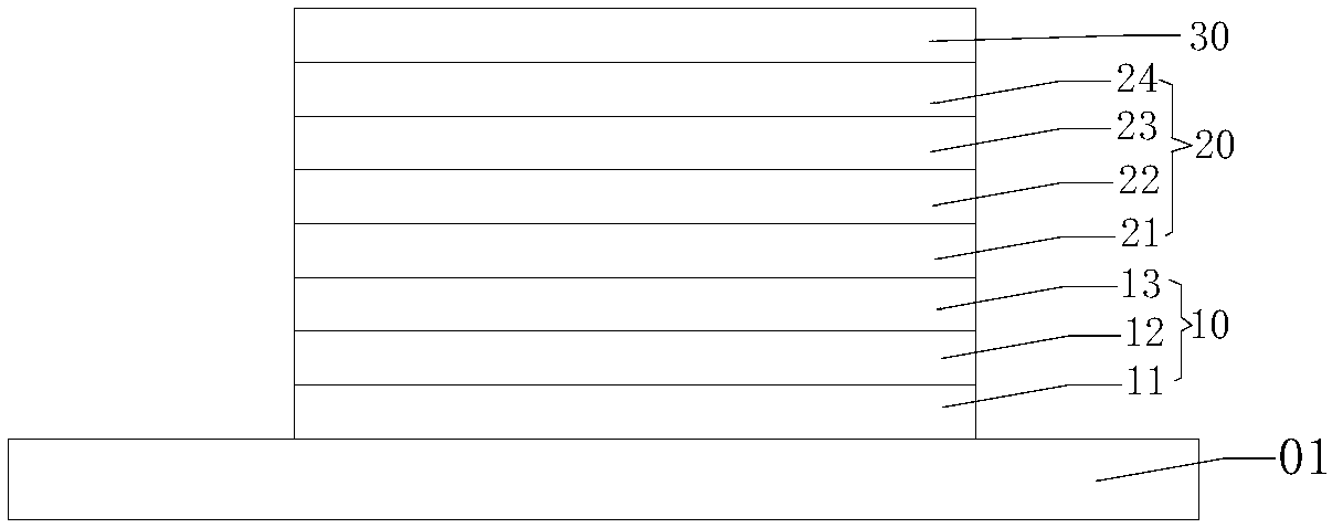
[0036] An embodiment, when the light emitting diode structure is such as figure 1 When shown, include the following steps:

[0037] Step S01. Deposit an interlayer composite anode 10 on the surface of the base layer 01: deposit a first metal oxide layer 11 and a graphene layer 12 on the surface of the base layer 01, and deposit a second metal oxide on the surface of the graphene layer 12 after annealing layer 13;

[0038] Step S02. Prepare the light-emitting unit 20 and the cathode 30 sequentially on the outer surface of the anode 10: sequentially deposit the surface of the second metal o...

Embodiment 1

[0057] In this embodiment, the compound anode light-emitting diode includes a structure such as figure 1 shown, including sequentially bonded glass / MoO 3 (20nm) / Graphene(80nm) / MoO 3 (20nm) / PEDOT:PSS(40nm) / TFB(50nm) / quantum dot light-emitting layer(70nm) / ZnO(40nm) / Al(100nm).

[0058] The light-emitting diode of this embodiment is prepared according to the following method:

[0059] S11: Place the glass substrate 0 in acetone, washing solution, deionized water and isopropanol in sequence for ultrasonic cleaning, and each step of ultrasonic cleaning needs to last for about 15 minutes. After the ultrasound is completed, place the substrate in a clean oven to dry for later use;

[0060] S12: After the substrate is dried, deposit a layer of MoO on it 3 Metal oxide 11, then, deposit a layer of graphene layer 12 on it, put it on the heating stage of 150 ℃ and heat for 15min, after the above-mentioned substrate includes the layer of graphene cooling, deposit a layer of graphene on ...

Embodiment 2

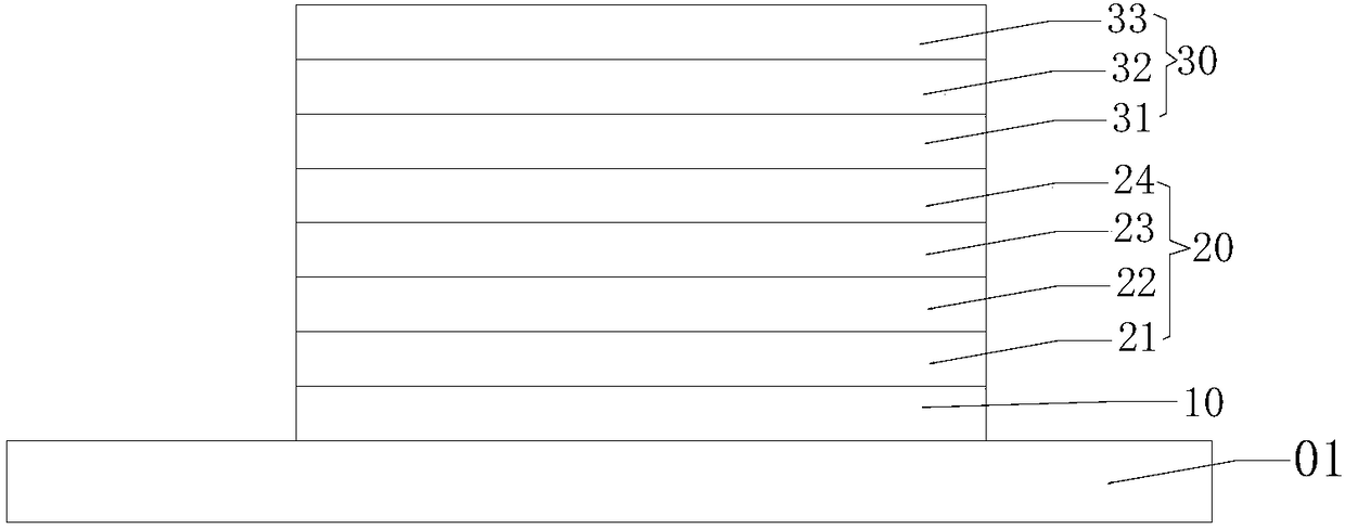
[0064] In this embodiment, the compound anode light-emitting diode includes a structure such as figure 1 shown, including sequentially bonded glass / MoO 3 (50nm) / Graphene(50nm) / WO 3 (10nm) / TFB(80nm) / quantum dot light-emitting layer (40nm) / ZnO(40nm) / Al(100nm).

[0065] The light-emitting diode of this embodiment refers to the preparation method of Embodiment 1 according to the following method.


PUM

PropertyMeasurementUnit
thicknessaaaaaaaaaa
thicknessaaaaaaaaaa
thicknessaaaaaaaaaa

Abstract

The present invention discloses a light emitting diode and a preparation method thereof, and an application thereof. The light emitting diode comprises an anode, a cathode and a light emitting unit combined between the anode and the cathode, the anode comprises a first metallic oxide layer, a graphene layer and a second metallic oxide layer combined in a stack mode in order, and the first metallicoxide layer or the second metallic oxide layer and the light emitting unit are combined in a stack mode. The anode included in the light emitting diode is a composite sandwich construction to achieveimprovement of the light take-out efficiency of the light emitting diode to increase the photoelectric efficiency and the electrical stability and the mechanical stability of the anode and ensure thelife stability of the light emitting diode. The preparation method of the light emitting diode ensures the electrical stability and the mechanical stability of the prepared light emitting diode, andthe application of the light emitting diode comprises application in a display screen or solid state illumination lamps and lanterns.

Description

technical field [0001] The invention belongs to the field of display technology, and in particular relates to a light-emitting diode, a preparation method thereof, a display screen or a solid-state lighting fixture. Background technique [0002] In recent years, with the rapid development of display technology, light-emitting diodes (QLEDs) that use semiconductor materials as light-emitting layers have attracted extensive attention. [0003] Due to their size-tunable optoelectronic properties, semiconductors have been widely used in light-emitting diodes, solar cells, and bioluminescent labels. After more than 20 years of development of synthesis technology, people have been able to synthesize various high-quality nanomaterials, and their photoluminescence efficiency can reach more than 85%. Light-emitting diodes (QLEDs) as light-emitting layers are promising light sources for next-generation displays and solid-state lighting due to their size-tunable luminescence, narrow l...

Claims


Application Information

Patent Timeline
Patent Type & Authority Applications(China)
IPC IPC(8): H01L51/52H01L51/56
CPCH10K50/81H10K50/826H10K50/852H10K71/00
Inventor 刘佳曹蔚然梁柱荣
Owner TCL CORPORATION
Why Eureka
Try Eureka