Ceramic chip antenna and preparation method thereof

A ceramic antenna and chip technology, applied in the field of ceramic antennas, can solve the problems of lack of interface bonding and separation, achieve excellent interface bonding, avoid air oxidation, and ensure antenna performance

Pending Publication Date: 2019-03-01
SHANGHAI AMPHENOL AIRWAVE COMM ELECTRONICS CO LTD
View PDF7 Cites 2 Cited by
  • Summary
  • Abstract
  • Description
  • Claims
  • Application Information

AI Technical Summary

Problems solved by technology

However, general experience shows that as the thickness of the metal layer increases, the difference between different metal la...

Method used


Image

  • Ceramic chip antenna and preparation method thereof
  • Ceramic chip antenna and preparation method thereof

Examples


preparation example Construction

[0052] A method for preparing the above-mentioned chip ceramic antenna includes the following steps:

[0053] S1) According to the material and size requirements of the ceramic base, the blank of the ceramic base is prepared by tape casting, punching and cutting processes;

[0054] S2) According to the material and thickness requirements of the first metal circuit, the first metal circuit is printed on the blank of S1 by a screen printing process, and sintered, to obtain the first metal circuit attached The ceramic base;

[0055] S3) According to the material and thickness requirements of the second metal circuit, any one of chemical vapor deposition, magnetron sputtering, electron beam evaporation deposition, electroplating, and electroless plating is used on the surface of the first metal circuit in S2 Preparing the second metal circuit;

[0056] S4) According to the material of the third metal circuit, the third metal circuit is prepared on the surface of the second metal circuit ...

Embodiment 1

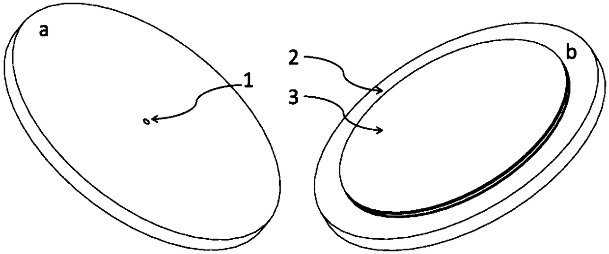
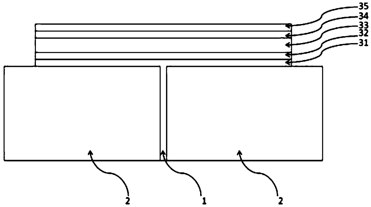
[0062] A structure design of a chip ceramic antenna, such as figure 1 , figure 2 Shown, including ceramic base and metal circuit:

[0063] among them,

[0064] The material of the ceramic base 2 is preferably alumina;

[0065] The metal circuit 3 is attached to the outer surface of the ceramic base 2 and the position of the via hole 1, wherein the metal circuit layer on the outer surface serves as the main body of the ceramic antenna, and the metal circuit located in the via hole serves as a circuit conduction function;

[0066] The metal circuit 3 has a multi-layer structure. According to the distance from the ceramic base, they are sequentially labeled as the first metal circuit 31, the second metal circuit 32, the third metal circuit 33, the fourth metal circuit 34, and the fifth metal circuit. 35;

[0067] The material of the first metal circuit 31 is preferably tungsten, and the thickness of the first metal circuit is preferably 1.5um;

[0068] The material of the second metal ci...

Embodiment 2

[0073] A method for preparing the chip ceramic antenna described in Example 1. It includes the following steps:

[0074] S1) According to the material of the ceramic base is preferably alumina and the size requirements, the green body of the ceramic base is prepared by casting, punching and cutting processes;

[0075] S2) According to the requirements that the material of the first metal circuit is preferably tungsten and the thickness is 1.5um, the first metal circuit is printed on the blank of the ceramic base described in S1 by a screen printing process, and high-temperature sintering is performed in an air environment , Sintering temperature is 1650℃, holding time is 2h;

[0076] S3) According to the requirement that the material of the second metal circuit is preferably chromium and the thickness is 0.5um, the second metal circuit is prepared on the surface of the first metal circuit in S2 by using a magnetron sputtering process;

[0077] S4) According to the requirement that th...


PUM

PropertyMeasurementUnit
Thicknessaaaaaaaaaa
Thicknessaaaaaaaaaa
Thicknessaaaaaaaaaa

Abstract

The invention discloses a ceramic chip antenna. Metal circuits are attached to the outer surface of a ceramic base and a via hole formed in the ceramic base, the metal circuit positioned on the outersurface serves as a ceramic antenna body, the metal circuit positioned at the via hole serves as a circuit functioning in conduction, the metal circuits comprise a first metal circuit, a second metalcircuit, a third metal circuit, a fourth metal circuit and a fifth metal circuit, the first metal circuit is selected from high-temperature-resistant tungsten, molybdenum and platinum, the third metalcircuit is selected from copper, silver, chromium, iron and cobalt with high conductivity, the second metal circuit is arranged between the first metal circuit and the third metal circuit and used for transition, and the fourth metal circuit and the fifth metal circuit are arranged on an outer layer and used for protection and welding. As a plurality of metal circuits are designed, the ceramic base and the metal circuits can be subjected to a co-firing process to form the ceramic chip antenna, cost is controlled, metal materials with excellent conductivity can be adopted, and antenna performances are ensured.

Description

Technical field [0001] The invention belongs to the technical field of ceramic antennas, and particularly relates to a structure design of a chip ceramic antenna and a preparation method thereof. Background technique [0002] For those skilled in the art, although it is common to choose ceramics as the antenna base, there are still problems to be solved. For example, there are many types of commonly used ceramics, and people are obviously more inclined to choose low-cost materials, such as zirconia, alumina and other common high-temperature sintered ceramics. Then, a metal circuit is prepared on the zirconia and alumina base by a suitable preparation method, and the metal circuit is used as the main body of the antenna. In various preparation methods, the co-firing process is used to subject the metal circuit and the ceramic matrix to high-temperature sintering, which helps to ensure an excellent interface combination between the two, while controlling the cost. However, the si...

Claims


Application Information

Patent Timeline
IPC IPC(8): C04B35/622C04B41/90C04B35/10H01Q1/38
CPCH01Q1/38C04B35/10C04B35/622C04B41/009C04B41/52C04B41/90C04B41/5133C04B41/5144C04B41/522C04B41/5127C04B41/524C04B41/5116
Inventor 吴昊曹海强
Owner SHANGHAI AMPHENOL AIRWAVE COMM ELECTRONICS CO LTD
Why Eureka
Try Eureka