
Three-dimensional packaging method with surface protection effect

A packaging method, a three-dimensional technology, applied in semiconductor/solid-state device manufacturing, electrical components, circuits, etc., can solve problems such as chip packaging failure, molding module failure, surface coating peeling off, etc., to achieve good insulation isolation, compact internal structure, The effect of protective metal plating

Active Publication Date: 2019-03-01
ZHUHAI ORBITA CONTROL ENG CO LTD
View PDF4 Cites 0 Cited by
  • Summary
  • Abstract
  • Description
  • Claims
  • Application Information

AI Technical Summary

Problems solved by technology

On the one hand, during the transportation, handling and use of the module, scratches will inevitably occur on the surface of the module, which will easily cause the surface coating of the module to be damaged and fall off, or to be damaged due to exposure, which will eventually cause the failure of the molded module and the failure of the chip package
On the other hand, since the metal plating layer interconnecting the upper and lower layers is exposed on the surface of the forming module, it is easily affected by moisture, pollutants, etc., resulting in a decrease in the insulation strength between the metal plating layers on the surface of the forming module, and eventually a short circuit failure occurs

Method used


Image

  • Three-dimensional packaging method with surface protection effect
  • Three-dimensional packaging method with surface protection effect
  • Three-dimensional packaging method with surface protection effect

Examples


Embodiment Construction

[0027] The specific embodiments of the present invention will be further described in detail below in conjunction with the accompanying drawings.

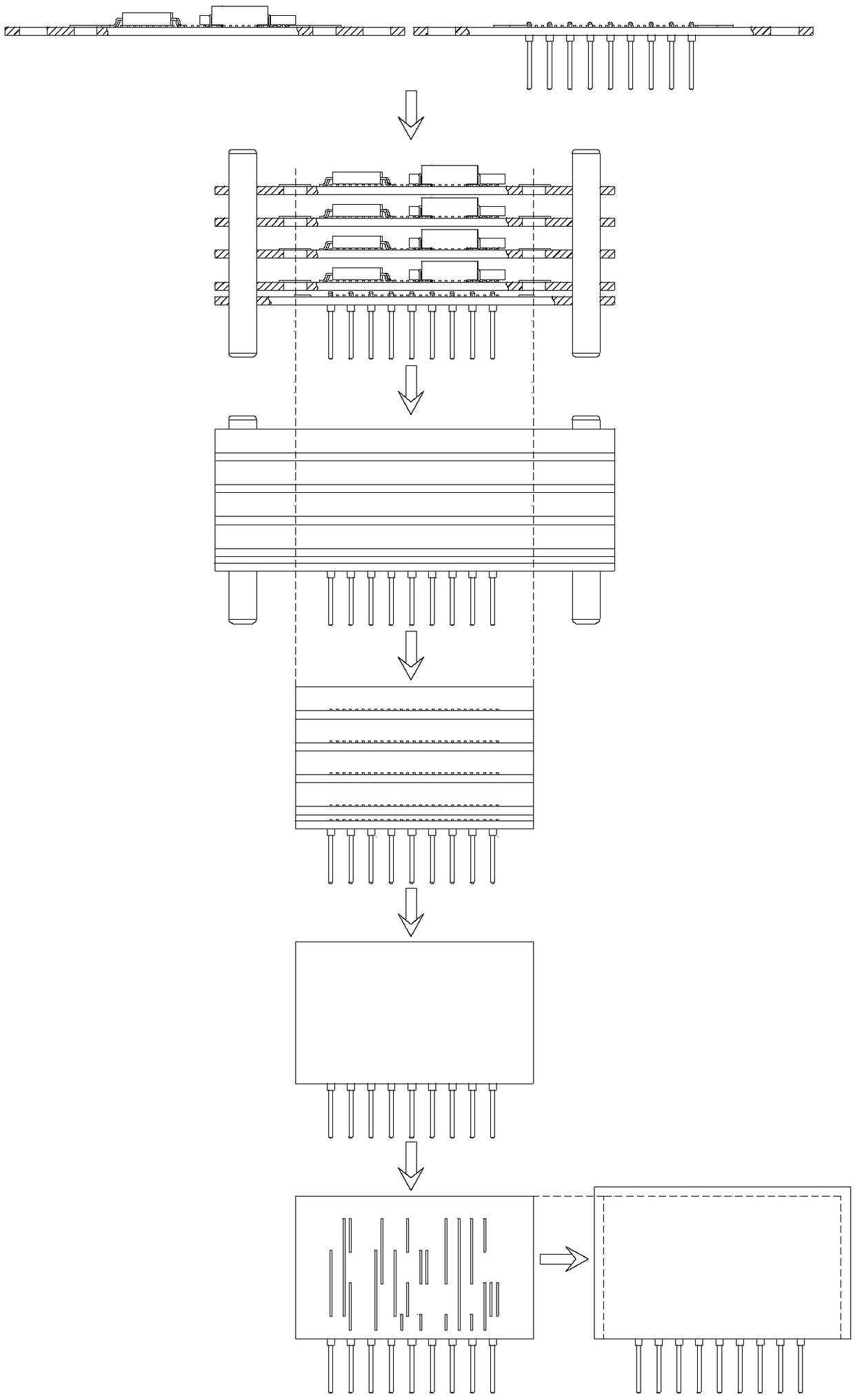
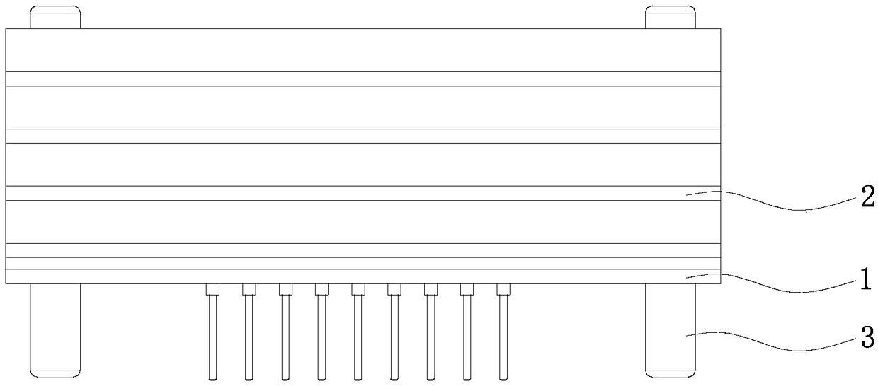
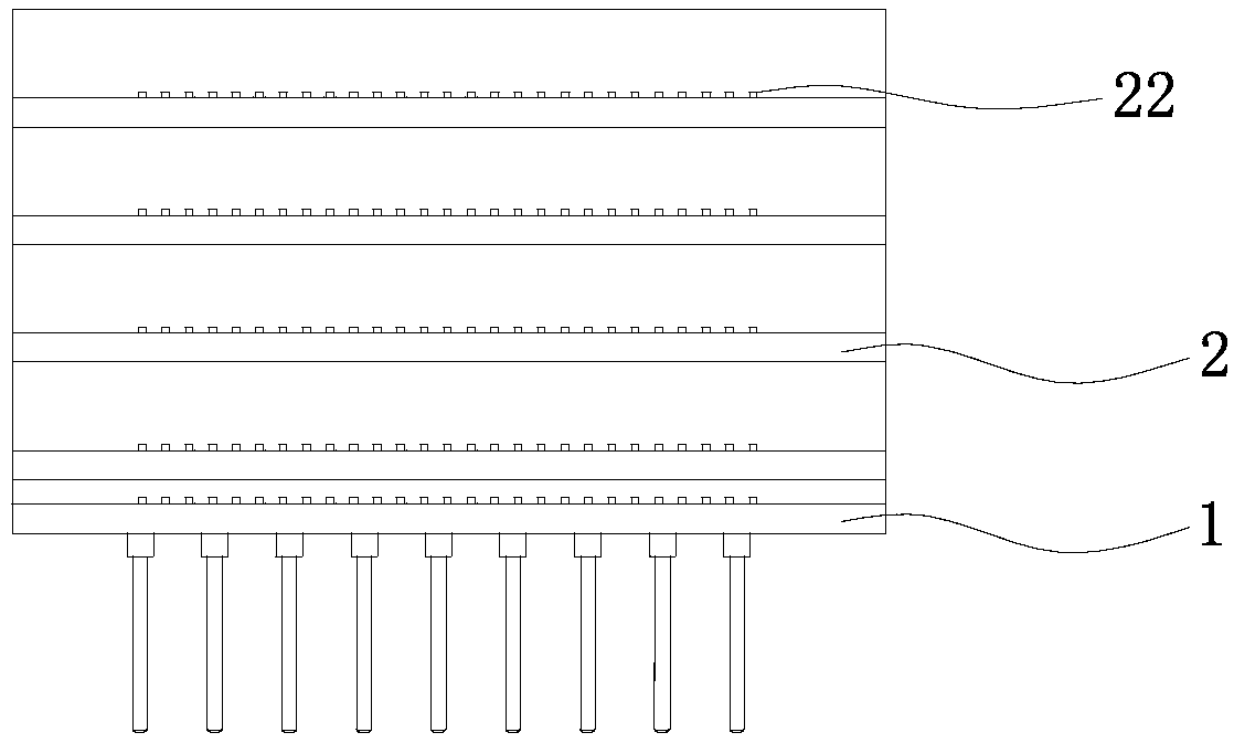
[0028] Such as Figure 1 to Figure 5 As shown, a vertical interconnection method for three-dimensional packaging includes the following steps:

[0029] Step a, electrical installation, the PCB board is divided into the middle part and the outside along the radial direction, the component 21 is assembled to the middle part of the PCB board, the outside of the PCB board is milled and drilled to form a slot 23 passing through the upper and lower ends, and the upper end of the slot 23 is assembled with an electrical connection component 21 The lead bridge 22, the positioning hole is milled and drilled on the PCB board to obtain the laminated board 2; the pins 11 are clamped on the jig, and one end of several pins 11 is connected through resin potting to obtain a socket with several pins 11 The base plate 1, the lead bridge 22 electric...


PUM


Abstract

The invention discloses a three-dimensional packaging method with a surface protection effect. An element and a lead bridge are assembled to a PCB; one ends of a plurality of pins are connected through resin pouring and sealing to obtain a bottom plate; laminated plates and the bottom plate are arranged on a jig; the laminated plates are arranged in a layered mode in the vertical direction up anddown; resin is poured and sealed between every two adjacent layers of plates, and after the resin is solidified and formed, cutting is carried out according to the designed size of a chip, and the section of the laminated plate lead bridge is exposed out of the side surface; the side surface is subjected to metal plating, and a metal plating layer is engraved, and then line connecting and formingare performed; and surface painting is carried out to form the side surface of a module III, and the top surface is painted. The chip obtained by packaging is compact in internal structure, high in electrical connection and high in insulation isolation of all layers; and relatively high outer layer hardness, reliability, long-term stability, acid and alkali resistance, cold and hot impact resistance and vacuum temperature resistance are achieved, so that the chip can be well applied to aerospace.

Description

technical field [0001] The invention relates to packaging technology, in particular to a three-dimensional packaging method for surface protection. Background technique [0002] In the miniaturized three-dimensional packaging module realized by the existing technology, the electrical interconnection of the upper and lower layers is realized by the metal coating on the surface of the molding module after laser engraving. The metal coating is completely exposed on the simulated surface, and the thickness of the coating is very thin, about 20um. On the one hand, during the transportation, handling and use of the module, scratches will inevitably occur on the surface of the module, which may easily cause the surface coating of the module to be damaged and fall off, or to be damaged due to exposure, and eventually lead to failure of the molded module and chip packaging. On the other hand, since the metal plating layer interconnecting the upper and lower layers is exposed on the s...

Claims


Application Information

Patent Timeline
Patent Type & Authority Applications(China)
IPC IPC(8): H01L21/50H01L21/56
CPCH01L21/50H01L21/56
Inventor 颜军黄小虎王烈洋颜志宇陈伙立骆征宾
Owner ZHUHAI ORBITA CONTROL ENG CO LTD
Learn More