SCR electrostatic protection device

An electrostatic protection and thyristor technology, which is applied in the direction of electric solid devices, electrical components, semiconductor devices, etc., can solve the problems of device burnout and high trigger voltage, and achieve higher P-well potential, lower trigger voltage, and higher secondary failure current. Effect

Active Publication Date: 2020-06-30
HUNAN UNIV
View PDF4 Cites 0 Cited by
  • Summary
  • Abstract
  • Description
  • Claims
  • Application Information

AI Technical Summary

Problems solved by technology

[0005] In view of the above situation, the purpose of the present invention is to solve the problem that the device is burned due to the high trigger voltage of the existing electrostatic protection device

Method used


Image

  • SCR electrostatic protection device
  • SCR electrostatic protection device
  • SCR electrostatic protection device

Examples


Embodiment Construction

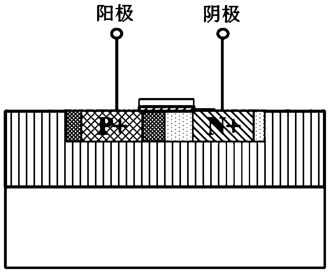
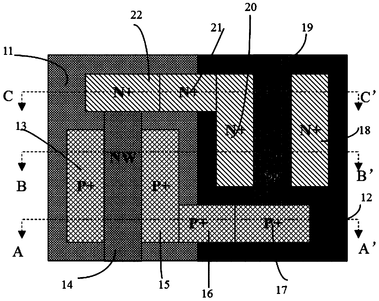
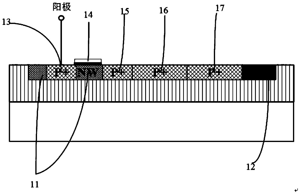
[0026] In order to make the above objects, features and advantages of the present invention more comprehensible, specific implementations of the present invention will be described in detail below in conjunction with the accompanying drawings. Several embodiments of the invention are shown in the drawings. However, the present invention can be embodied in many different forms and is not limited to the embodiments described herein. Rather, these embodiments are provided so that the disclosure of the present invention will be thorough and complete.

[0027] It should be noted that when an element is referred to as being “fixed on” another element, it may be directly on the other element or there may be an intervening element. When an element is referred to as being "connected to" another element, it can be directly connected to the other element or intervening elements may also be present. As used herein, the terms "vertical," "horizontal," "left," "right," "upper," "lower," a...


PUM


Abstract

The invention provides a silicon-controlled electrostatic protection device. The silicon-controlled electrostatic protection device comprises a substrate, an oxide buried layer, an N well and a P well, wherein a first P+ injection region, a first poly-silicon gate, a second P+ injection region and a fourth N+ injection region are arranged in the N well, a first N+ injection region, a second poly-silicon gate, a second N+ injection region and a fourth P+ injection region are arranged in the P well, the third P+ injection region and the third N+ injection region bridge at a junction between theN well and the P well, the first P+ injection region is connected with a positive electrode, the first N+ injection region is connected with a negative electrode, the first P+ injection region, the first poly-silicon gate, the second P+ injection region and the N well form a PMOS tube, and the first N+ injection region, the second poly-silicon gate, the second N+ injection region and the P well form an NMOS tube. The silicon-controlled electrostatic protection device has the advantages of low trigger voltage, high maintenance voltage, simple structure, high robustness and the like, is easy tointegrate and is suitable for electrostatic protection of the device and a circuit.

Description

technical field [0001] The invention relates to the technical field of electrostatic protection for integrated circuits, in particular to a thyristor electrostatic protection device. Background technique [0002] With the development of Moore's Law, the integration of chips has been continuously improved, and power consumption and performance have been greatly improved. However, when the bulk silicon technology develops to 28nm, the technical complexity and manufacturing cost increase greatly, and fully depleted silicon-on-insulator (FDSOI) emerges as the times require. Under the same technology node, FDSOI technology can effectively reduce the manufacturing process, reduce chip power consumption, improve product yield, and has strong radiation resistance. Due to its advantages in price, power consumption and performance, FDSOI has gradually become a mainstream technology in applications such as the Internet of Things. [0003] Electrostatic discharge (Electro Static Disch...

Claims


Application Information

Patent Timeline
Patent Type & Authority Patents(China)
IPC IPC(8): H01L27/02
CPCH01L27/0262H01L27/0266
Inventor 吴铭陈卓俊曾云彭伟吴志强
Owner HUNAN UNIV
Why Eureka
Try Eureka