Method for processing a layer structure and microelectromechanical component
A technology for processing layers, electrical devices, applied in the process of producing decorative surface effects, electrical components, piezoelectric/electrostrictive/magnetostrictive devices, etc.
- Summary
- Abstract
- Description
- Claims
- Application Information
AI Technical Summary
Problems solved by technology
Method used
Image

Examples
Embodiment approach
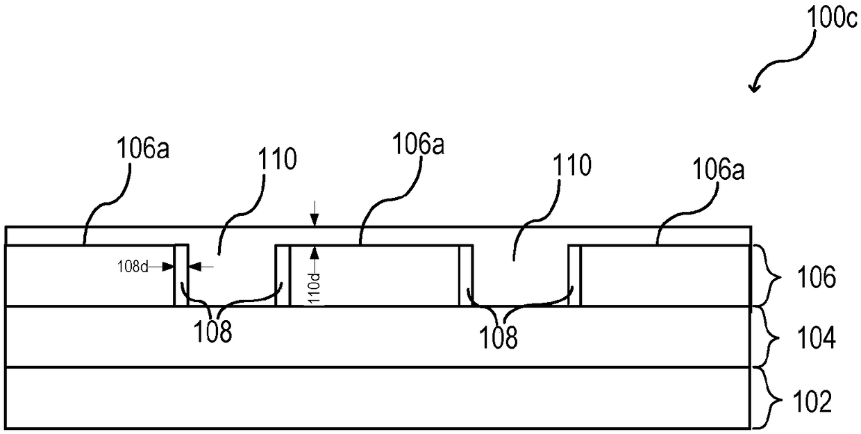
[0043] According to various implementations, the cover layer 110 may be formed (eg, directly) over the liner layer 108 . According to various embodiments, the capping layer 110 may be formed by means of chemical or physical vapor deposition, such as by means of PE-CVD, LP-CVD, SA-CVD, ALD, RTO, thermal evaporation, laser deposition, cathode sputtering, and the like.
[0044] According to various embodiments, the remaining space in the corresponding opening 106h may be filled by means of the cover layer 110 . Furthermore, the cover layer 110 can also be formed over the first side 106a of the second layer 106 (ie the surface facing away from the sacrificial layer 104) and optionally partially or completely cover the backing layer 108, for example as in Figure 1C as well as Figure 2B The schematic side view or cross-sectional view shown in.
[0045] According to various embodiments, the liner layer 108 may have an undoped oxide material, such as undoped silicon oxide (also kn...
example 1
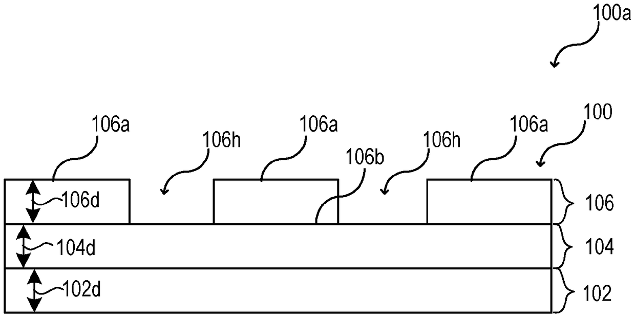
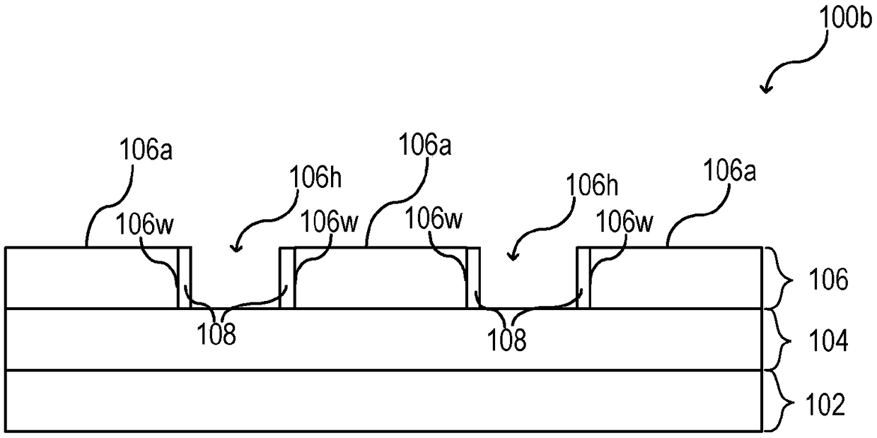
[0135] Example 1 is a method comprising: forming a layer structure 100 having a first layer 102, a sacrificial layer 104 disposed over the first layer, and a second layer 106 disposed over the sacrificial layer, wherein the second layer 106 having at least one opening 106h, wherein the at least one opening 106h extends from the first side 106a of the second layer 106 to the sacrificial layer 104; forming a liner layer 108 covering at least one inner wall 106w of the at least one opening 106h; in the liner layer 108 to form a capping layer 110, wherein the capping layer 110 at least partially extends into at least one opening 106h; A cavity 104 g is formed between the first layer 102 and the second layer 106 , wherein the etching rate of the etchant for the liner layer 108 is greater than that for the covering layer 110 .
[0136] Alternatively, Example 1 is a method for processing a carrier, the method comprising: forming a layer structure 100 having a first layer 102, a sacri...
Embodiment 13
[0151] Embodiment 13 is a microelectromechanical device 400, which has: a first layer 102 and a second layer 106 disposed on the first layer 102, wherein a cavity 104g is provided between the two layers 102, 106, and wherein the second The second layer 106 has a contact region 100k; a liner layer 108, which is disposed in the contact region 100k above the second layer 106, wherein the liner layer 108 has an undoped oxide material, and wherein the liner layer 108 has a thickness less than 50nm (eg less than 40nm or less than 30nm) layer thickness; cover layer 110, which is arranged in the contact region 100k above the pad layer 108, wherein the cover layer 110 has a doped oxide material, and wherein the layer thickness of the cover layer 110 Greater than the layer thickness of the liner layer 108, wherein the contact hole 424 extends through the liner layer 108 and the cover layer 110 to the second layer 106 to contact the surface portion 406a of the second layer 106; the conduc...
PUM
| Property | Measurement | Unit |
|---|---|---|
| thickness | aaaaa | aaaaa |
| thickness | aaaaa | aaaaa |
| thickness | aaaaa | aaaaa |
Abstract
Description
Claims
Application Information
 - R&D
- Intellectual Property
- Life Sciences
- Materials
- Tech Scout
- Unparalleled Data Quality
- Higher Quality Content
- 60% Fewer Hallucinations
Browse by: Latest US Patents, China's latest patents, Technical Efficacy Thesaurus, Application Domain, Technology Topic, Popular Technical Reports.
© 2025 PatSnap. All rights reserved.Legal|Privacy policy|Modern Slavery Act Transparency Statement|Sitemap|About US| Contact US: help@patsnap.com