Broad Spectrum Infrared Sensor Based on Piezoelectric Effect and Composite Plasmons

An infrared sensor and plasmon technology, applied in the field of infrared sensing, can solve the problems of limited range of material selection, increased process complexity, and limited number of stacked layers, and achieve the goal of overcoming the limited bandwidth of infrared radiation absorption and reliable infrared transmission. Sensitive performance and easy adjustment of absorption width

Active Publication Date: 2020-11-03
CHANGCHUN INST OF OPTICS FINE MECHANICS & PHYSICS CHINESE ACAD OF SCI
View PDF21 Cites 0 Cited by
  • Summary
  • Abstract
  • Description
  • Claims
  • Application Information

AI Technical Summary

Problems solved by technology

At present, multi-layer structure absorption is usually used to increase the absorption bandwidth, and the absorption band of different layers is used to widen the absorption bandwidth of the absorption layer. Specifically, it includes: using different materials to prepare the absorption layer, but this method is limited by the stress of material preparation, and the range of material selection is limited. And increasing the thickness of the absorbing layer will affect the performance of the infrared sensor; using a multi-layer micro-bridge structure, however, is limited by the difficulty of the process and the number of stacked layers is limited, so the absorption width is limited. In addition, this method greatly increases the process complexity and reduces the reliability of the infrared sensor. sex

Method used


Image

  • Broad Spectrum Infrared Sensor Based on Piezoelectric Effect and Composite Plasmons
  • Broad Spectrum Infrared Sensor Based on Piezoelectric Effect and Composite Plasmons
  • Broad Spectrum Infrared Sensor Based on Piezoelectric Effect and Composite Plasmons

Examples


Embodiment Construction

[0034] In order to understand the above-mentioned purpose, features and advantages of the present invention more clearly, the present invention will be further described in detail below in conjunction with the accompanying drawings and specific embodiments.

[0035] In the following description, many specific details are set forth in order to fully understand the present invention. However, the present invention can also be implemented in other ways different from those described here. Therefore, the protection scope of the present invention is not limited by the specific details disclosed below. EXAMPLE LIMITATIONS.

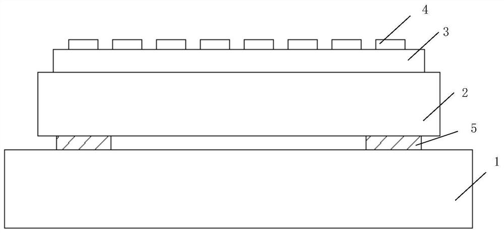
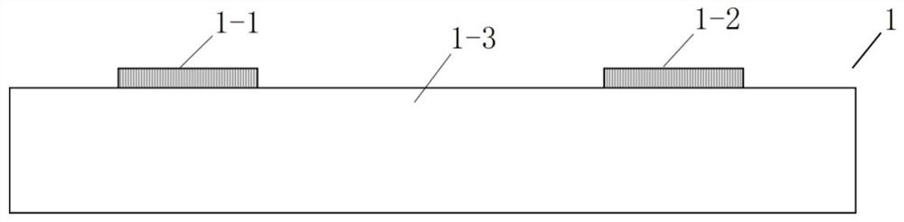
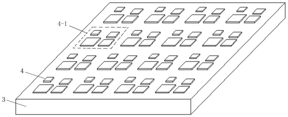
[0036] Wide-spectrum infrared sensors based on piezoelectric effect and composite plasmons, such as figure 1 As shown, the infrared sensor also includes a readout integrated circuit substrate 1 (also known as ROIC substrate), a microelectromechanical resonator 2, a dielectric layer 3 and a metal array layer 4, the readout integrated circuit substrate 1, the micr...


PUM


Abstract

The wide-spectrum infrared sensor based on piezoelectric effect and composite plasmon involves the field of infrared sensing technology, which solves the problems of low absorption rate and limited broadband absorption bandwidth in the prior art, including sequentially connected readout integrated circuits A substrate, a microelectromechanical resonator, a dielectric layer and a metal array layer. The metal array layer includes a plurality of metal units, and each metal unit is composed of at least three metal blocks of different sizes. The uncooled infrared sensor of the present invention realizes the enhanced absorption of the infrared spectrum by the uncooled infrared sensor by integrating the dielectric layer and the metal array layer on the surface of the FBAR, and the absorption rate is increased from 20% to more than 80%, and at the same time, broadband absorption is realized, and the production is simple and convenient. The infrared sensor has excellent sensing performance; integrated on the integrated readout circuit substrate through FBAR, etc., it can be integrated manufacturing, mass production, and low cost; it has the advantages of traditional uncooled infrared sensing, and at the same time has fast response and high sensing sensitivity .

Description

technical field [0001] The invention relates to the technical field of infrared sensing, in particular to a wide-spectrum infrared sensor based on piezoelectric effects and composite plasmons. Background technique [0002] According to the working temperature, infrared sensors are generally divided into two categories: cooling type and non-cooling type. Cooled infrared sensors are usually made of semiconductor materials. Using the photoelectric effect of some materials, the photosensitive material absorbs photons, causing changes in electrical parameters. In order to suppress hot carriers and noise, the operating temperature of the cooled infrared sensor is usually below 77K. It needs to be refrigerated by a refrigerator or liquid nitrogen, which will result in relatively large volume and weight, and relatively expensive prices. Uncooled infrared sensors are also called room temperature sensors, which can work at room temperature without refrigeration, so they have the ad...

Claims


Application Information

Patent Timeline
Patent Type & Authority Patents(China)
IPC IPC(8): G01J5/10G01J5/02
CPCG01J5/0205G01J5/0215G01J5/10
Inventor 梁中翥陶金孟德佳梁静秋秦余欣吕金光张宇昊秦正
Owner CHANGCHUN INST OF OPTICS FINE MECHANICS & PHYSICS CHINESE ACAD OF SCI
Why Eureka
Try Eureka