Silicon-based optical random waveform generation chip

An arbitrary waveform and optical technology, applied in the field of optical communication, to achieve the effect of large bandwidth, low power consumption, and small chip size

Active Publication Date: 2019-03-12
SHANGHAI JIAO TONG UNIV
View PDF5 Cites 11 Cited by
  • Summary
  • Abstract
  • Description
  • Claims
  • Application Information

AI Technical Summary

Problems solved by technology

Nevertheless, the current optical arbitrary waveform generation system still has many technical problems in terms of speed, power consumption, integration level, etc., waiting for researchers to overcome

Method used


Image

  • Silicon-based optical random waveform generation chip
  • Silicon-based optical random waveform generation chip
  • Silicon-based optical random waveform generation chip

Examples


Embodiment Construction

[0021] In order to further clarify the purpose, technical solution and core advantages of this solution, the present invention will be further described in detail below in conjunction with the accompanying drawings. This embodiment is carried out on the premise of the technical solution of the present invention, and the detailed implementation and operation process are given, but the protection scope of the present invention is not limited to the following embodiments.

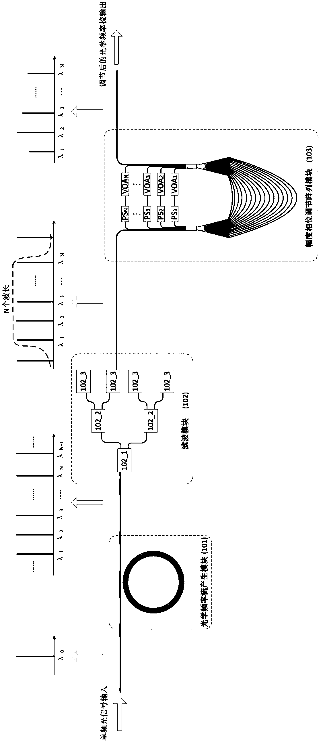
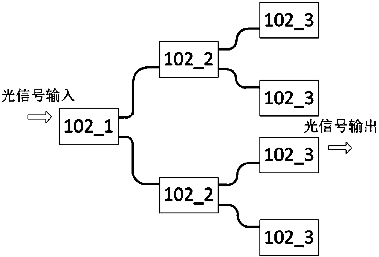
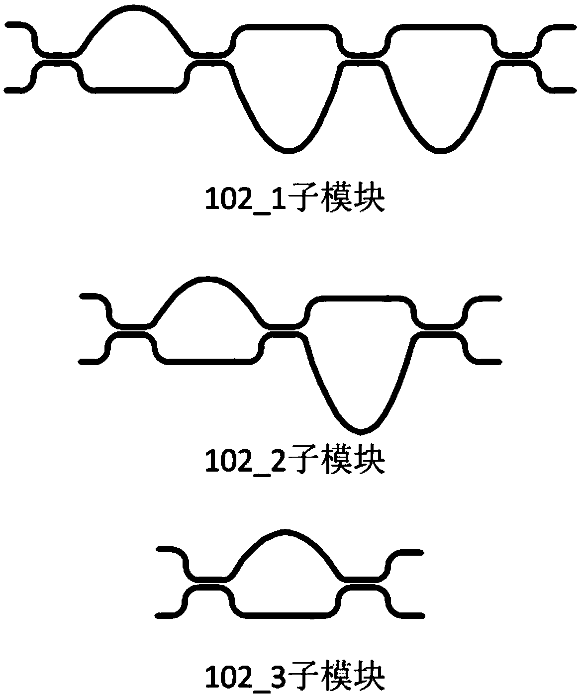
[0022] figure 1 It is a schematic diagram of the overall principle of the silicon-based optical arbitrary waveform generation chip of the present invention. Such as figure 1 As shown, the silicon-based optical arbitrary waveform generation chip of the present invention is divided into three parts according to functional characteristics: an optical frequency comb generation module 101 , a filtering module 102 and an amplitude and phase adjustment array module 103 .

[0023] An optical signal of a single frequ...


PUM


Abstract

The invention discloses a silicon-based optical random waveform generation chip. The chip comprises an optical frequency comb generation module, a filter module and an amplitude phase regulating arraymodule. The optical frequency comb generation module is composed of a tunable micro-ring resonator, the filter module is composed of cascading Mach-Zehnder interferometers, and the amplitude phase regulating array module is composed of a feedback array waveguide optical grating, a variable optical attenuator and a phase shifter. Any waveform generation inside the optical frequency region can be achieved, the chip has the advantages of being small in size, low in consumption, high in stability and the like, and the key role can be brought into play in an optical communication network and system.

Description

technical field [0001] The invention belongs to the field of optical communication, in particular to a silicon-based optical arbitrary waveform generating chip. Background technique [0002] With the rapid increase of services such as modern communication networks and computer networks, the amount of data is increasing explosively, and people have higher requirements for bandwidth. In order to meet the increasing demand for information capacity, the optical communication network will remain the core of the next generation network. Due to the continuous increase of optical communication capacity, the next-generation all-optical network has put forward higher requirements for active devices, especially light sources. Ultrashort pulse light source is one of the most dynamic research topics in the field of laser technology and high-speed optical communication applications, and has a huge application prospect. In practical applications, we not only need to generate high-quality...

Claims


Application Information

Patent Timeline
Patent Type & Authority Applications(China)
IPC IPC(8): G02B6/12H04B10/50H04B10/516
CPCG02B6/12004G02B6/12019H04B10/501H04B10/5161
Inventor 周林杰刘源彬陆梁军陈建平
Owner SHANGHAI JIAO TONG UNIV
Why Eureka
Try Eureka