Process integrated method for improving multistep polycrystalline silicon etching damage of split gate structure flash memory

An integrated method and polysilicon technology, applied in the direction of electrical components, electrical solid devices, circuits, etc., can solve the problems of silicon dioxide film being easily etched through, active area etching damage, economic loss, etc., to reduce etching damage The risk of avoiding etching damage in the active area and the effect of improving stability

Active Publication Date: 2019-03-12
SHANGHAI HUALI MICROELECTRONICS CORP
View PDF5 Cites 0 Cited by
  • Summary
  • Abstract
  • Description
  • Claims
  • Application Information

AI Technical Summary

Problems solved by technology

[0007] The present invention is aimed at the existing multi-step multi-step polysilicon total dry etching and wet cleaning amount is too much, if the active area with high risk of etching damage is not processed, the original surface of the active area The silicon dioxide film will be easily etched through, causing etching damage in the active area, wafer scrapping, causing huge economic losses and other defects Provide a process integration method for improving the multi-step polysilicon etching damage of split-gate flash memory

Method used


Image

  • Process integrated method for improving multistep polycrystalline silicon etching damage of split gate structure flash memory
  • Process integrated method for improving multistep polycrystalline silicon etching damage of split gate structure flash memory
  • Process integrated method for improving multistep polycrystalline silicon etching damage of split gate structure flash memory

Examples


Embodiment Construction

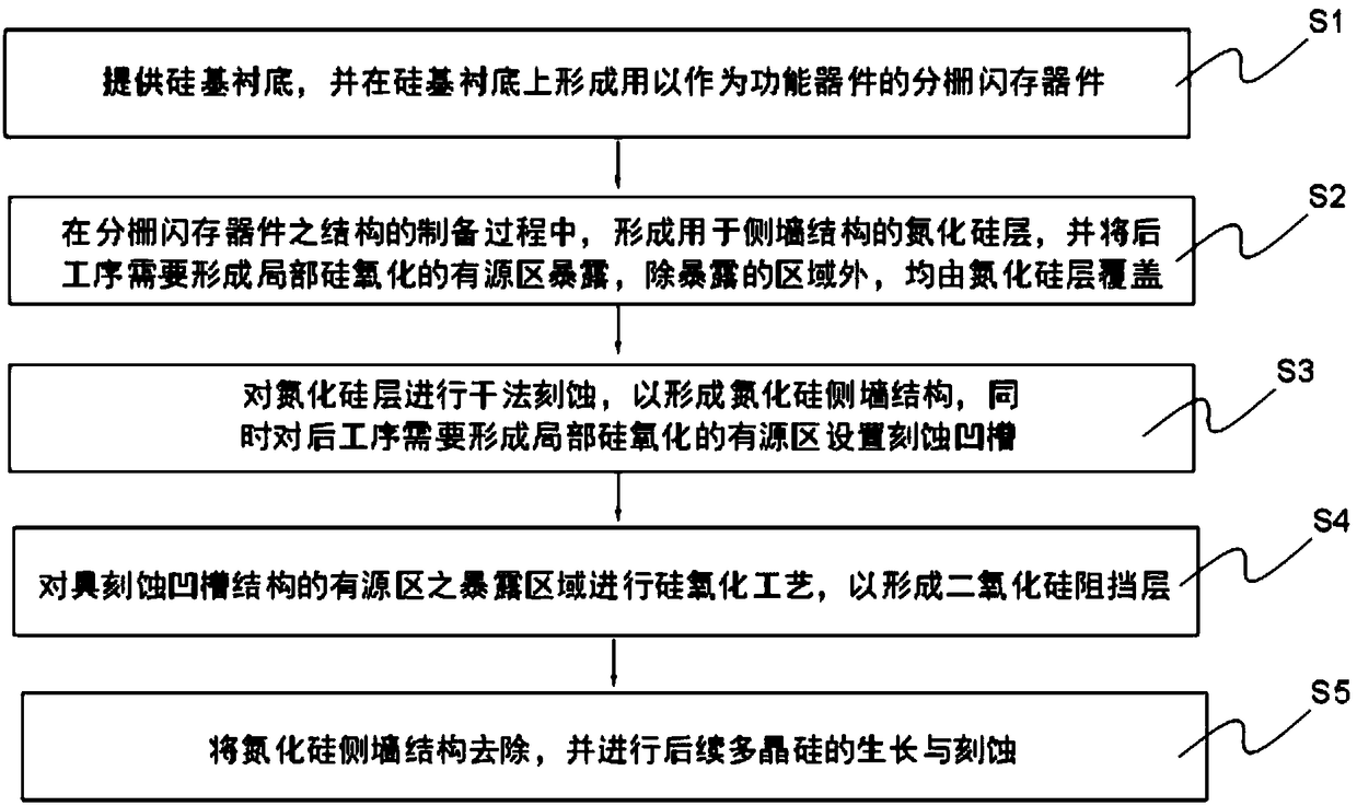
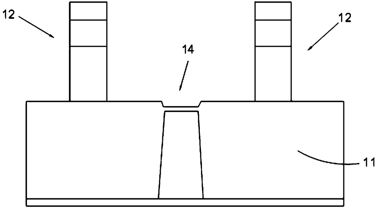
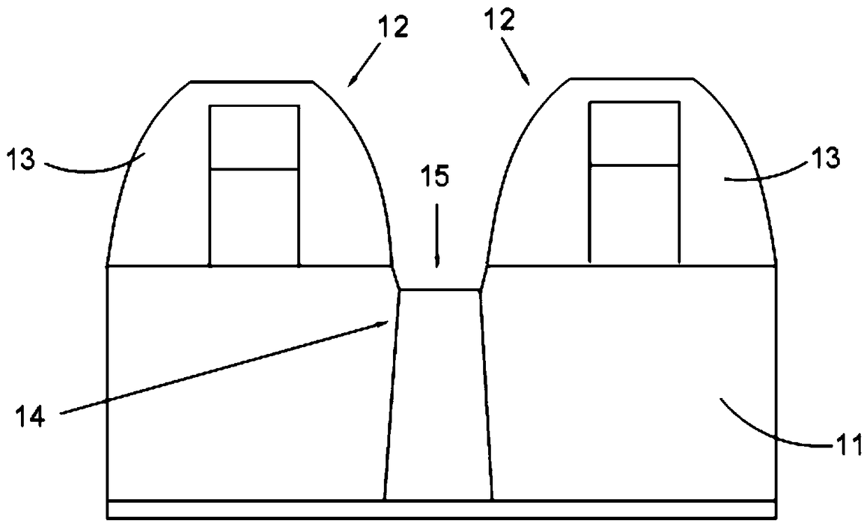
[0026] In order to illustrate the technical content, structural features, achieved goals and effects of the present invention in detail, the following will be described in detail in conjunction with the embodiments and accompanying drawings.

[0027] Due to its advantages of high density, low price, and electrical programmability and erasability, flash memory has been widely used as the best choice for non-volatile memory applications. At present, the floating-gate non-volatile flash memory is mainly divided into two types according to its structure: ETOX flash memory and split-gate flash memory. The main difference between the two lies in the programming / erasing method and cell structure. The programming / erasing method of ETOX flash memory is: channel hot electron injection / FN tunneling method, and the split-gate flash memory is: source channel hot electron Injection / field-enhanced poly-to-poly FN tunneling method; structurally, ETOX flash memory is a stacked gate structure, ...


PUM

PropertyMeasurementUnit
depthaaaaaaaaaa
thicknessaaaaaaaaaa
depthaaaaaaaaaa

Abstract

The invention discloses a process integrated method for improving a multistep polycrystalline silicon etching damage of a split gate structure flash memory. The method comprises the following steps: step S1: providing a silicon substrate and forming a split gate flash memory device thereon; step S2: forming a silicon nitride layer in a device preparation process, and exposing an active area that needs to form local silicon oxidation in a subsequent process; step S3: performing dry etching on the silicon nitride layer to form a silicon nitride sidewall structure, and forming an etching groove in the active area; step S4: performing a silicon oxidation process on the exposed area of the active area to form a silicon dioxide barrier layer; and step S5: removing the silicon nitride sidewall structure, and performing subsequent polycrystalline silicon growing and etching processes. According to the process integrated method, the active area etching damage generated by multistep polycrystalline silicon etching in the split gate structure flash memory can be effectively prevented, the stability of the whole process is improved, and the process is simple and is conveniently embedded into the existing process procedures; and furthermore, the risk that the active area has the etching damage is greatly reduced, the process technological requirements of FAB are met and the process integrated method is deserved to be promoted and applied.

Description

technical field [0001] The invention relates to the technical field of semiconductor manufacturing, in particular to a process integration method for improving multi-step polysilicon etching damage of flash memory with divided gate structure. Background technique [0002] Due to its advantages of high density, low price, and electrical programmability and erasability, flash memory has been widely used as the best choice for non-volatile memory applications. At present, the floating-gate non-volatile flash memory is mainly divided into two types according to its structure: ETOX flash memory and split-gate flash memory. The main difference between the two lies in the programming / erasing method and cell structure. The programming / erasing method of ETOX flash memory is: channel hot electron injection / FN tunneling method, and the split-gate flash memory is: source channel hot electron Injection / field-enhanced poly-to-poly FN tunneling method; structurally, ETOX flash memory is a...

Claims


Application Information

Patent Timeline
Patent Type & Authority Applications(China)
IPC IPC(8): H01L27/11521H01L21/28
CPCH01L29/40114H10B41/30
Inventor 胡涛张磊田志王奇伟陈昊瑜
Owner SHANGHAI HUALI MICROELECTRONICS CORP
Why Eureka
Try Eureka