HEMT device containing high-dielectric coefficient medium block

A high dielectric coefficient, dielectric block technology, applied in the direction of electrical components, semiconductor devices, circuits, etc., can solve the problems of limiting the maximum output power of HEMT devices and reducing the breakdown electric field, and achieve high breakdown voltage and small on-resistance , to meet the effect of working voltage and output power

Active Publication Date: 2019-03-12
UNIV OF ELECTRONICS SCI & TECH OF CHINA
View PDF3 Cites 9 Cited by
  • Summary
  • Abstract
  • Description
  • Claims
  • Application Information

AI Technical Summary

Problems solved by technology

However, in the working state of the device, due to the concentrated electric field distribution between the gate and the drain, it is easy to generate an electric field peak in this area, resulting in a decrease in the breakdown electric field, which limits the maximum output power of the HEMT device

Method used


Image

  • HEMT device containing high-dielectric coefficient medium block
  • HEMT device containing high-dielectric coefficient medium block
  • HEMT device containing high-dielectric coefficient medium block

Examples


Embodiment Construction

[0030] The technical solution of the present invention will be described in detail below in conjunction with the accompanying drawings and specific embodiments.

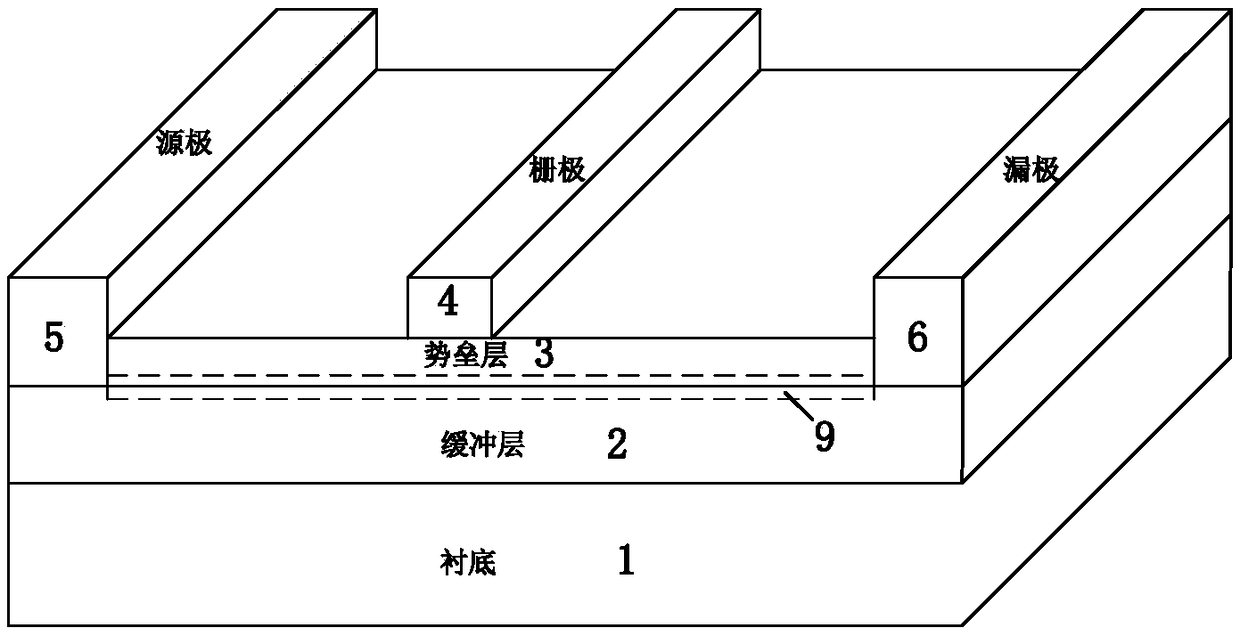
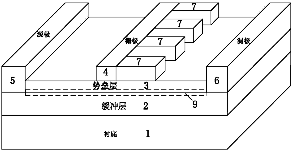
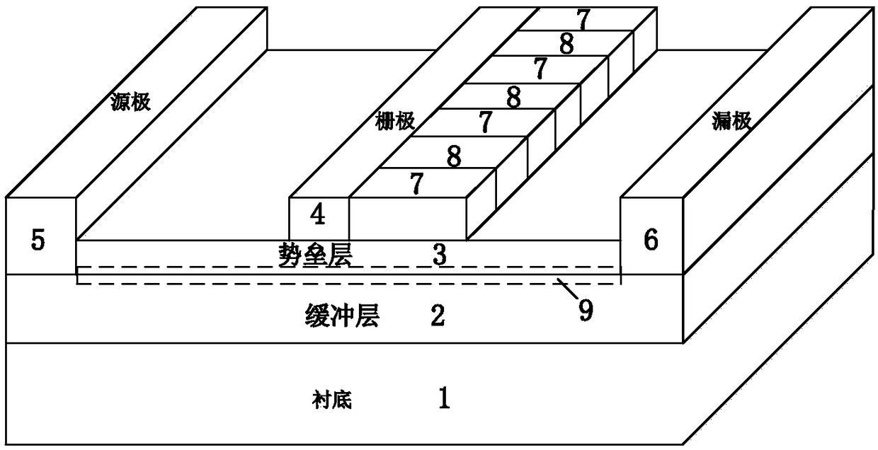
[0031] A HEMT device with a high dielectric coefficient dielectric block proposed by the present invention comprises a substrate 1, a buffer layer 2, a barrier layer 3, a gate 4, a source 5 and a drain 6, and the substrate 1 is sequentially arranged with a buffer layer 2 and barrier layer 3, a two-dimensional conductive channel 9 is formed at the interface between the barrier layer 3 and the buffer layer 2; the source electrode 5 and the drain electrode 6 are respectively arranged on both sides of the HEMT device and are connected to the two-dimensional conductive channel 9 to form an ohmic contact; the gate 4 is arranged between the source 5 and the drain 6, and the gate 4 is located on the barrier layer 3 to form a Schottky contact with the barrier layer 3; the barrier layer 3 is located on the gate 4 and The regio...


PUM


Abstract

The invention discloses a HEMT device containing high-dielectric coefficient medium blocks, and belongs to the technical field of the semiconductor. The HEMT device comprises a substrate, a buffer layer, a barrier layer, a grid electrode, a source electrode and a drain electrode; the buffer layer and the barrier layer are orderly arranged on the substrate, and a two-dimensional conducting channelis formed at an interface of the barrier layer and the buffer layer; the source electrode and the drain electrode are respectively arranged at two sides of the HEMT device and form ohmic contact withthe two-dimensional conducting channel; the grid electrode is arranged between the source electrode and the drain electrode, and the grid electrode is located on the barrier layer and the Schottky contact is formed on the barrier layer; multiple high-dielectric coefficient medium blocks are arranged at a region between the grid electrode and the drain electrode on the barrier layer; multiple high-dielectric coefficient medium blocks are connected with the grid electrode and extend along a grid drain direction, the grid electrode and multiple high-dielectric coefficient medium blocks form a comb-finger shaped structure; the high-dielectric coefficient medium blocks do not directly connect with the drain electrode, and the dielectric coefficient is greater than the dielectric coefficient ofthe barrier layer. The HEMT device provided by the invention has the feature of being high in breakdown voltage, and can satisfy the application with high working voltage and output power.

Description

technical field [0001] The invention belongs to the technical field of semiconductors and relates to a high electron mobility transistor (HEMT), in particular to a HEMT device containing a high dielectric coefficient dielectric block. Background technique [0002] In the field of radio frequency and power integrated circuits, the frequency, withstand voltage, on-resistance and other characteristics of the device are important performance indicators that determine the characteristics of the circuit. The requirements for these features are also getting higher and higher. Among RF power devices, compared with other power devices, HEMT (High Electron Mobility Transistor) devices have the characteristics of ultra-high speed, low power consumption, and low noise (especially at low temperature), which greatly meets the needs of ultra-high-speed computers and Due to the special requirements of signal processing, satellite communication and other applications, HEMT devices are widel...

Claims


Application Information

Patent Timeline
Patent Type & Authority Applications(China)
IPC IPC(8): H01L29/778H01L29/06
CPCH01L29/0607H01L29/778
Inventor 罗谦孟思远文厚东姜玄青
Owner UNIV OF ELECTRONICS SCI & TECH OF CHINA
Why Eureka
Try Eureka