Semiconductor device assembly method and production line thereof

An assembly method and semiconductor technology, applied in semiconductor/solid-state device manufacturing, electrical components, conveyor objects, etc., can solve the problems of unguaranteed quality, easy deviation of parts, high labor intensity, etc., and reduce the amount of solder paste Unevenness, reduce labor intensity, and improve production efficiency

Pending Publication Date: 2019-03-15
乐山希尔电子股份有限公司
View PDF0 Cites 2 Cited by
  • Summary
  • Abstract
  • Description
  • Claims
  • Application Information

AI Technical Summary

Problems solved by technology

In the production process, it needs to be assembled and welded by multiple parts. The traditional process is manually assembled in graphite molds. This method is inefficient and labor-intensive. Employees are prone to strain on shoulders, necks, arms, waists, etc. , when employees are tired or not careful, it is easy to have quality problems such as missing materials, reversed materials, and damaged materials
The traditional process uses solid solder sheet as the welding material, which causes the parts to be easily misaligned and the quality cannot be guaranteed

Method used


Image

  • Semiconductor device assembly method and production line thereof
  • Semiconductor device assembly method and production line thereof
  • Semiconductor device assembly method and production line thereof

Examples


Embodiment 1

[0047] As one of the most basic implementations of the present invention, this embodiment discloses a semiconductor device assembly method and its production line. The semiconductor device assembly method includes the following steps:

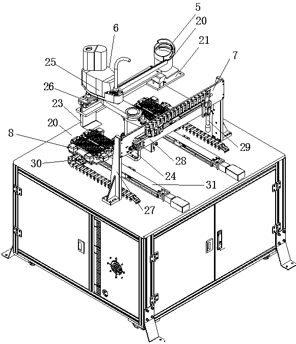
[0048] 1) Automatic assembly of lead wires: first install the graphite box on the lead wire installation device 8, then pour the lead wires into the vibrating plate 22, start the automatic lead wire assembly equipment through the PLC controller, the automatic lead wire assembly equipment automatically completes the lead wire assembly, and then put the stone cartridge removal;

[0049] 2) Dispensing of lead wires and assembly of the lower connecting piece: first install the graphite box that has completed the lead wire assembly on the positioning tool 12 of the graphite box, and then shake the lower connecting piece into the connecting piece sieve plate 11 and install it The connecting piece sieve plate 11 of the connecting piece is installed on...

Embodiment 2

[0055] As a preferred embodiment of the present invention, this embodiment discloses a semiconductor device assembly method and its production line. The semiconductor device assembly method includes the following steps:

[0056] 1) Automatic assembly of lead wires: first install the graphite box on the lead wire installation device 8, then pour the lead wires into the vibrating plate 22, start the automatic lead wire assembly equipment through the PLC controller, the automatic lead wire assembly equipment automatically completes the lead wire assembly, and then put the stone cartridge removal;

[0057] 2) Dispensing of lead wires and assembly of the lower connecting piece: first install the graphite box that has completed the lead wire assembly on the positioning tool 12 of the graphite box, and then shake the lower connecting piece into the connecting piece sieve plate 11 and install it The connecting piece sieve plate 11 of the connecting piece is installed on the lead dispe...


PUM


Abstract

The invention discloses a semiconductor device assembly method and a production line thereof, and relates to the technical field of semiconductor device production. The semiconductor device productionline comprises an automatic lead assembly device, a lead dispensing and lower connection piece assembly device, a chip assembly device and an upper connection piece assembly device. The method comprises the following steps: 1), automatic assembly of leads; 2), lead dispensing and lower connection piece assembly; 3), chip tinning; 4), lower connection piece assembly. The method is high in efficiency, is accurate in positioning and is low in damage rate.

Description

technical field [0001] The invention belongs to the technical field of semiconductor device production, and in particular relates to a method for assembling a semiconductor device and a production line thereof. Background technique [0002] Semiconductor devices are widely used in rail transit, home appliances, new energy, power supplies, frequency converters, consumer electronics, computers and peripherals, network communications, automotive electronics, LEDs and other fields. In the production process, it needs to be assembled and welded by multiple parts. The traditional process is manually assembled in graphite molds. This method is inefficient and labor-intensive. Employees are prone to strain on shoulders, necks, arms, waists, etc. , When employees are tired or careless, it is also prone to quality problems such as missing materials, reversed materials, and damaged materials. The traditional process uses solid solder sheet as the welding material, which causes the com...

Claims


Application Information

Patent Timeline
IPC IPC(8): H01L21/67H01L21/683H01L21/677
CPCH01L21/67011H01L21/67121H01L21/67126H01L21/67144H01L21/6715H01L21/67155H01L21/67703H01L21/6838
Inventor 邓华鲜
Owner 乐山希尔电子股份有限公司
Why Eureka
Try Eureka