Silicon-based integrated optical adjustable delay line based on optical phased array

一种光相控阵、集成光学的技术,应用在光学、光学元件、光波导光导等方向,能够解决不利高速系统应用、限制器件工作带宽、延时调节范围小等问题,达到调节灵活、结构紧凑、控制简单的效果

Active Publication Date: 2019-03-19
SHANGHAI JIAOTONG UNIV
View PDF8 Cites 15 Cited by
  • Summary
  • Abstract
  • Description
  • Claims
  • Application Information

AI Technical Summary

Problems solved by technology

[0007] The first method has relatively large limitations, because the effective refractive index of the medium is related to the refractive index of the device material and the waveguide structure, and the range that can be changed is generally small, and the optical absorption loss of the material itself should also be considered when selecting the medium, so This method is hardly used
[0008] The second method has the best adjustability and can realize continuous adjustment. Using the principles of electro-optic effect, thermo-optic effect or carrier dispersion effect of materials, material dispersion or waveguide dispersion can be realized, but this method also has limitations, which is relatively Large dispersion is often accompanied by signal distortion, which limits the working bandwidth of the device and is not conducive to the application in high-speed systems, so the delay adjustment range achieved by this method is often small
However, since the amount of delay is proportional to the length of the waveguide, due to problems such as loss and system complexity, it is impossible to increase the size of the device indefinitely in practical applications. It is necessary to make the delay adjustment range and loss of the device through reasonable design. optimize

Method used


Image

  • Silicon-based integrated optical adjustable delay line based on optical phased array
  • Silicon-based integrated optical adjustable delay line based on optical phased array
  • Silicon-based integrated optical adjustable delay line based on optical phased array

Examples


Embodiment Construction

[0034] In order to further clarify the purpose, technical solution and core advantages of this solution, the present invention will be further described in detail below in conjunction with the accompanying drawings and embodiments. Please note that the following specific examples are for illustrative purposes only, and are not intended to limit the present invention. At the same time, as long as the technical features involved in the various embodiments do not constitute a conflict with each other, they can be combined with each other.

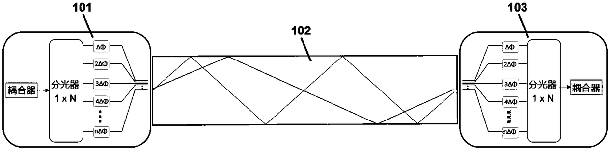
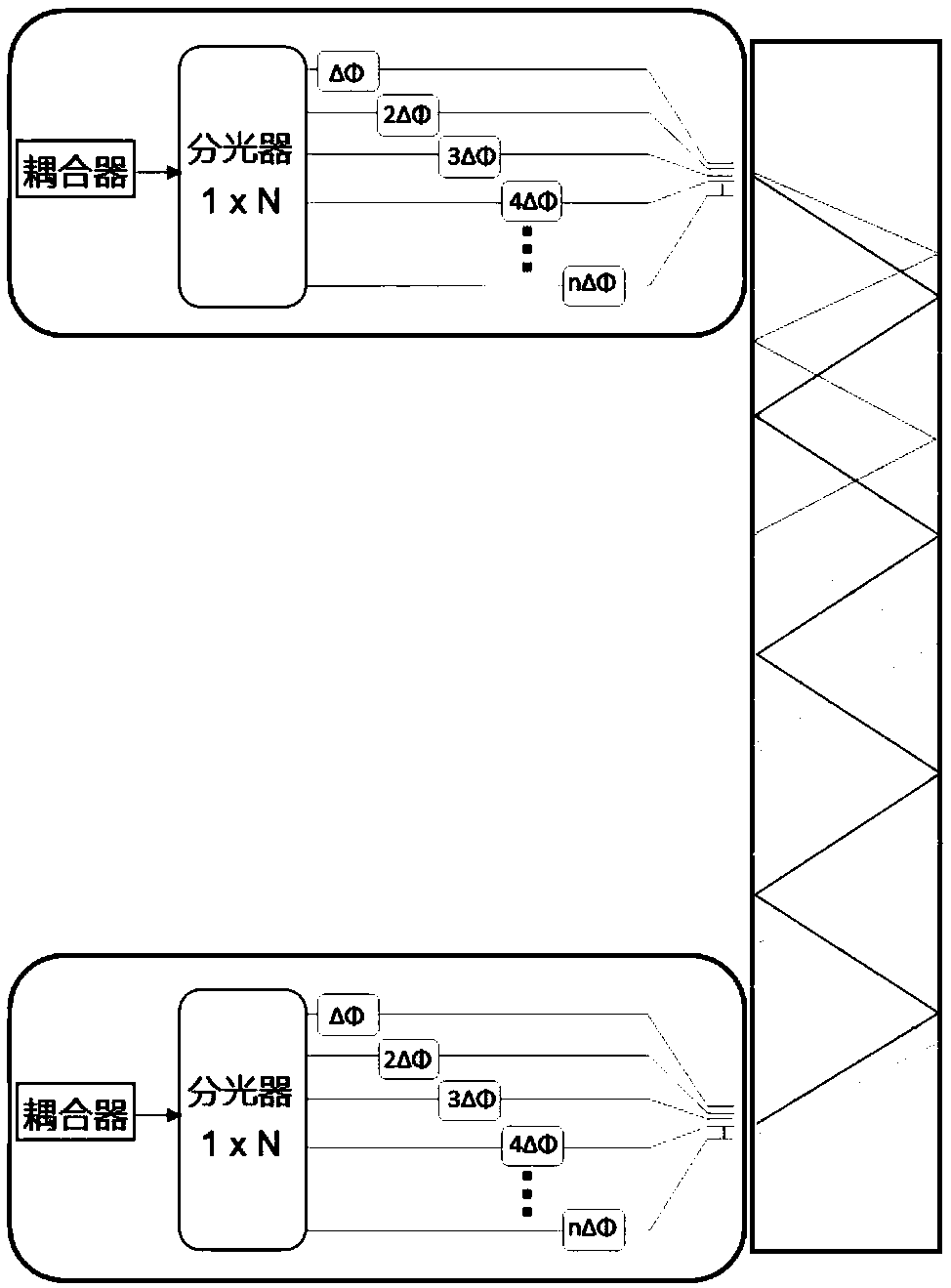
[0035] refer to figure 1 , figure 2 As shown, the integrated adjustable delay line based on optical phased array of the present invention is mainly divided into three parts according to functional characteristics: optical phased array transmitting unit (101), planar waveguide transmission unit (102), optical phased array receiving unit (103); The described optical phased array emitting unit (101) is sequentially composed of a coupler, a cas...


PUM


Abstract

The invention relates to a silicon-based integrated optical adjustable delay line based on an optical phased array. The silicon-based integrated optical adjustable delay line sequentially comprises anoptical phased array transmitting unit, a platy waveguide transmitting unit and optical phased array receiving units. Through the optical phased array transmitting unit, a phase shift is adopted foradjusting and controlling the phase difference between channels to change far-field interference faculae in order to form a directional beam, correspondingly the incident angle of an optical signal entering a platy waveguide is adjusted and controlled, and the length of a propagation path of the optical signal is thus changed; finally, the optical signal is received through the corresponding optical phased array receiving unit, and different delay amounts are obtained. Specifically, the silicon-based integrated optical adjustable delay line can obtain the large adjustable delay amounts, has the advantages of being simple in structure, easy to control, high in integration level and the like, and has a high application value in the aspects of optical communication, microwave photons, signalprocessing and the like.

Description

technical field [0001] The invention belongs to the field of optical delay / optical buffer. By combining the optical phased array transmitting and receiving unit with the transmission waveguide, the angle-adjustable optical path is formed with the help of the optical phased array, and different delays are obtained through multiple total reflection transmissions in the waveguide, thereby realizing an integrated adjustable optical delay. timeline. Background technique [0002] Data buffering is a key unit in the optical communication network, which can avoid channel network conflicts, improve the throughput of network nodes, and reduce the packet loss rate. In the next-generation all-optical switching network (such as packet switching), the performance index of data buffering is required to be higher. Early all-optical switching networks used electrical random-access memory (RAM, random-access memory,) to access information. The optical switching speed of this method is limit...

Claims


Application Information

Patent Timeline
Patent Type & Authority Applications(China)
IPC IPC(8): G02B6/12G02B6/124
CPCG02B6/12009G02B6/124G02B2006/12038G02F1/292G02B2006/12107
Inventor 周林杰单文胜许维翰陆梁军陈建平刘娇
Owner SHANGHAI JIAOTONG UNIV
Why Eureka
Try Eureka