Large-view-field imaging device

An imaging device and a large field of view technology, which is applied in semiconductor devices, electric solid state devices, electrical components, etc., can solve the problems of high cost and long design cycle, and achieve the effect of low cost, simple manufacturing process and large field of view

Active Publication Date: 2021-08-24
BEIJING UNIV OF TECH
View PDF3 Cites 1 Cited by
  • Summary
  • Abstract
  • Description
  • Claims
  • Application Information

AI Technical Summary

Problems solved by technology

These large-scale detector array sizes are the most direct way to increase the field of view of imaging devices, but this method has a long design cycle, high cost, and physical limitations

Method used


Image

  • Large-view-field imaging device
  • Large-view-field imaging device
  • Large-view-field imaging device

Examples


Embodiment Construction

[0030] In order to make the purpose, technical solutions and advantages of the embodiments of the present invention clearer, the technical solutions in the embodiments of the present invention will be clearly and completely described below in conjunction with the drawings in the embodiments of the present invention. Obviously, the described embodiments It is a part of embodiments of the present invention, but not all embodiments. Based on the embodiments of the present invention, all other embodiments obtained by persons of ordinary skill in the art without making creative efforts belong to the protection scope of the present invention.

[0031] In the description of the present invention, it should be noted that the terms "center", "upper", "lower", "left", "right", "vertical", "horizontal", "inner", "outer" etc. The indicated orientation or positional relationship is based on the orientation or positional relationship shown in the drawings, and is only for the convenience of...


PUM


Abstract

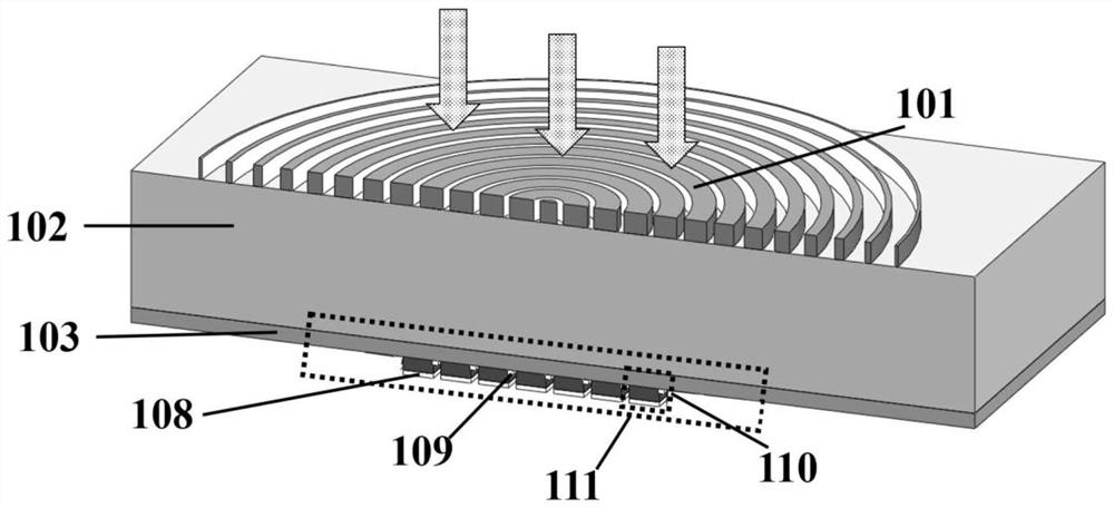
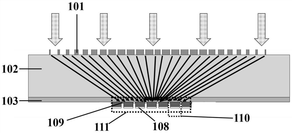
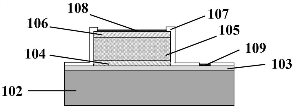
The invention, which belongs to the technical field of photoelectric detection, discloses a large-view-field imaging device comprising a surface microstructure, a substrate layer, a buffer layer, a pixel array and a passivation layer. The pixel array comprises at least one pixel unit, and each pixel unit comprises an n + type doping layer, an absorption layer and a p + type doping layer; an n + type electrode penetrating through the passivation layer is led out from the buffer layer of the substrate layer, and a p + type electrode penetrating through the passivation layer is led out from the p + type doping layer; the surface microstructure can change the transmission path of light, so that incident light signals are converged through the focusing effect of the surface microstructure, the converged light signals are transmitted to the pixel array to generate photo-induced electron hole pairs capable of freely moving, and electric signals are formed under the application of bias voltage. The large-view-field imaging device has the advantages of being large in imaging view field, small in pixel unit size and the like, and the pixel units can be applied to visible light imaging, infrared imaging and ultraviolet imaging according to different materials.

Description

technical field [0001] The invention relates to the technical field of photoelectric detection, in particular to an imaging device with a large field of view. Background technique [0002] Photodetector is an important optoelectronic device that converts incident radiation signal into electrical signal output. Imaging devices form observable images through photoelectric conversion of photodetectors, and are widely used in military and civilian fields. [0003] Photoelectric imaging devices occupy a very important position in military and civilian applications, and are widely used in the fields of investigation, tracking, early warning, and confrontation. Visible light imaging technology has been popularized in military (reconnaissance, early warning, tracking, etc.), high-speed image transmission and processing aerospace, multi-spectral hyperspectral remote sensing, medical medical diagnosis and testing, etc. Products of visible light imaging and infrared imaging devices a...

Claims


Application Information

Patent Timeline
Patent Type & Authority Applications(China)
IPC IPC(8): H01L31/0232H01L31/105H01L27/144H01L27/146
CPCH01L31/02327H01L31/105H01L27/1443H01L27/1446H01L27/14643
Inventor 李冲李占杰杨帅张琛辉李巍泽温哲
Owner BEIJING UNIV OF TECH
Why Eureka
Try Eureka