
Screening method for diffusion barrier layer of thermoelectric component
A screening method and barrier layer technology are applied in the field of screening of diffusion barrier materials of thermoelectric components, which can solve the problems of long R&D cycle, low R&D efficiency and high cost of barrier materials, and achieve the effect of fast and low-cost screening
- Summary
- Abstract
- Description
- Claims
- Application Information
AI Technical Summary
Problems solved by technology
Method used
Image

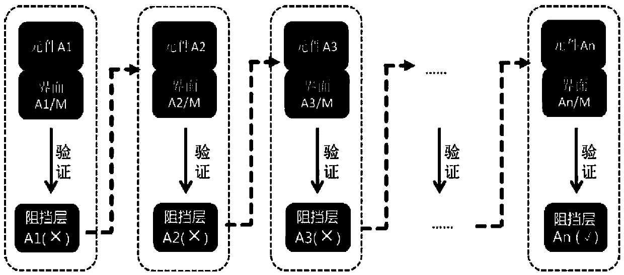
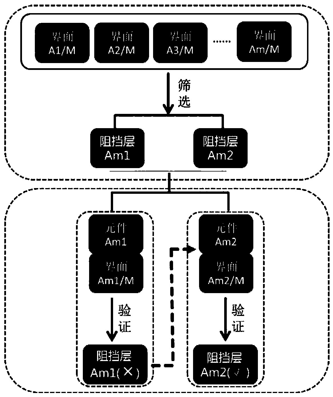
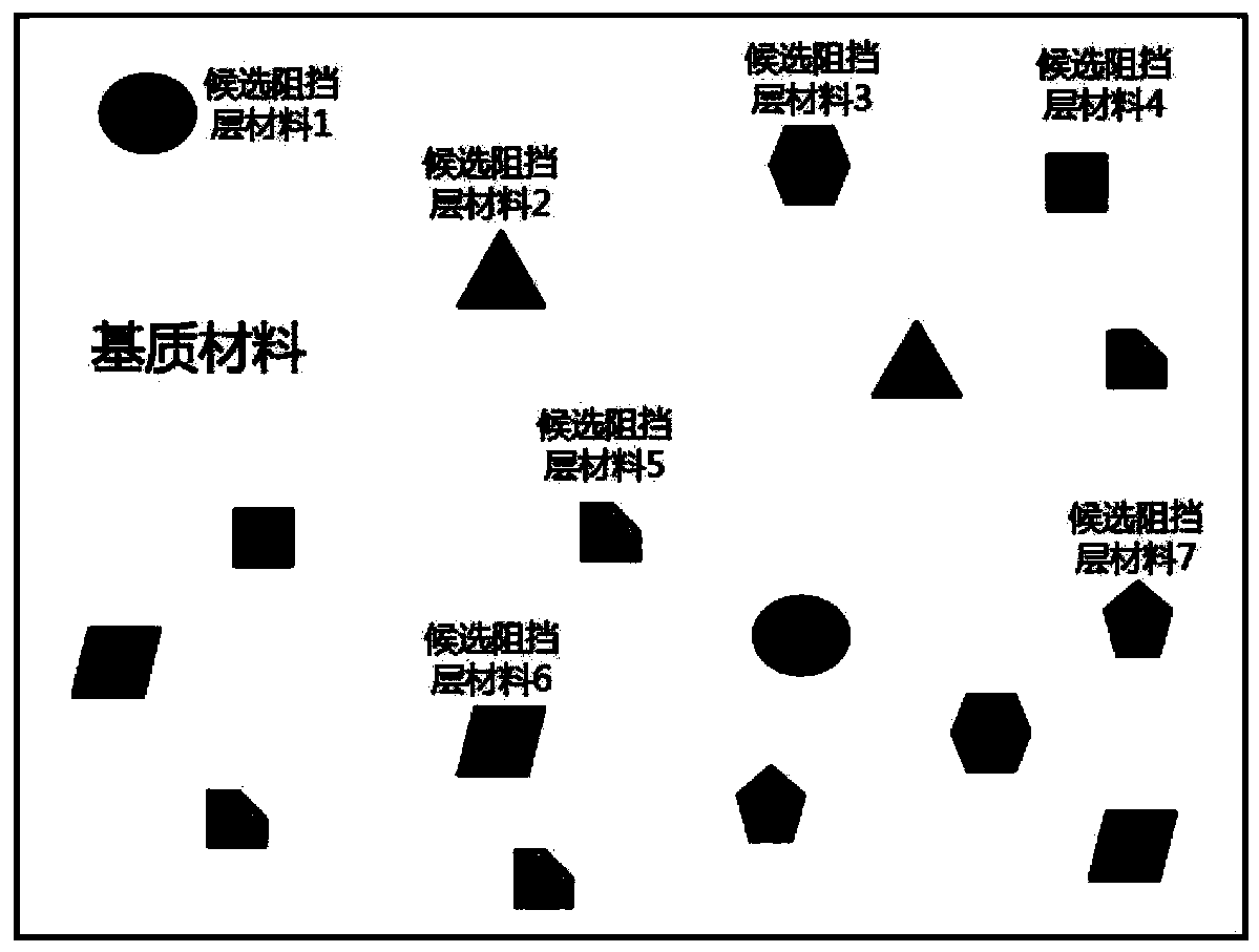
Examples
Embodiment 1
[0054] Take the component as Yb 0.3 co 4 Sb 12 n-type skutterudite powder (n-SKD) 2.5g, take Ti(4N, 45um), Zr(3N, 75um), Hf(3N, 75um), V(3N, 75um), Nb(4N, 45um) , Ta, Cr (3N5, 150um), Mo (3N, 75um), W (3N, 75um) powders, each 0.02g, mixed with n-SKD powder evenly. Put the mixed powder into a graphite mold with a diameter of 12.7mm, put the mold into an SPS sintering system, and conduct spark plasma rapid sintering under vacuum: the chamber pressure is <10Pa, the sintering pressure is 64MPa, the heating rate is 80°C / min, and the sintering temperature is 620°C , the holding time is 10 min, the cooling rate is 60 °C / min, and the temperature is lowered to 200 °C and then cooled in the furnace to obtain a densified co-sintered sample, which contains the interface between the above nine candidate barrier particles and the n-SKD matrix material. The above-mentioned co-sintered samples were sealed in a vacuum quartz tube and heated at 650°C for 2 days. The surface of the heat-dura...
Embodiment 2
[0058] Take the component as Yb 0.3 co 4 Sb 12 Put 4g of n-type skutterudite powder (n-SKD) into a graphite mold with a diameter of 12.7mm, put the mold into an SPS sintering system, and perform discharge plasma rapid sintering under vacuum: chamber pressure -3 Pa, continue pumping, and start to heat up at the same time. After 30 minutes, the chamber temperature reaches 200°C, keep it warm for half an hour, then feed high-purity Ar, and sputter the Mo target with 1.5kW power for 40 minutes under the chamber pressure of 1.1Pa. After the sputtering is over, the equipment is turned off, the sample is cooled with the furnace, and the chamber temperature is lower than 70°C, then the cabin is opened and the sample is taken out. The sample was cut by wire cutting to obtain the structure Mo / Yb 0.3 co 4 sb 12 The thermoelectric element and the corresponding macroscopic interface. The above-mentioned components were sealed in a vacuum quartz tube, and heated at 650°C for 2 days. T...
PUM
 Abstract
Description
Claims
Application Information