LDMOS device and manufacturing method thereof

A technology of devices and drift regions, applied in the field of laterally diffused metal oxide semiconductor devices and their preparation, to achieve the effects of reducing forward conduction resistance, improving and reducing depth

Inactive Publication Date: 2019-03-29
HUAIAN IMAGING DEVICE MFGR CORP
View PDF4 Cites 1 Cited by
  • Summary
  • Abstract
  • Description
  • Claims
  • Application Information

AI Technical Summary

Problems solved by technology

In LDMOS devices, the drift region used to bear the withstand voltage needs to be doped with a low concentration, but on the other hand, in order to reduce the on-resistance of the LDMOS device in forward conduction, the drift region as a current channel is required to have a high doping concentration. , which creates a contradiction between on-resistance and breakdown voltage

Method used


Image

  • LDMOS device and manufacturing method thereof
  • LDMOS device and manufacturing method thereof
  • LDMOS device and manufacturing method thereof

Examples


Embodiment 1

[0079] The technical solution of the LDMOS device of the present invention will be described in detail below in conjunction with the accompanying drawings.

[0080] In this embodiment, the direction from the source to the drain or from the drain to the source is defined as the width direction, and the direction from the upper surface of the substrate to the lower surface or from the lower surface of the substrate to the upper surface is defined as the depth direction.

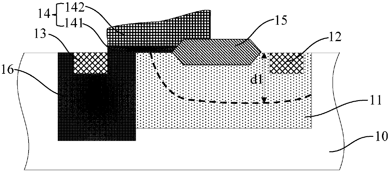
[0081] Such as figure 2 As shown, a schematic cross-sectional structure diagram of the LDMOS device of this embodiment is shown. Please note that in this embodiment, the N-type LDMOS device is used as an example for illustration, but those skilled in the art can understand that the present invention is also fully applicable to the P-type LDMOS device, only the conductivity type of each doped region Just reverse it.

[0082] Please refer to figure 2 , this embodiment provides an LDMOS device, the LDMOS devi...

Embodiment 2

[0107] The technical solution of the manufacturing method of the LDMOS device of the present invention will be described in detail below in conjunction with the accompanying drawings.

[0108] As described in Example 1, in this embodiment, the preparation method of an N-type LDMOS device is used as an example for illustration, but those skilled in the art can understand that the present invention is also fully applicable to the preparation method of a P-type LDMOS device. It is only necessary to invert the conductivity type of each doped region.

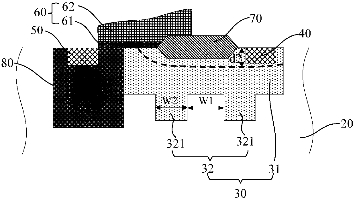
[0109] see Figure 4 and Figure 5 , first proceed to step S1), providing a P-type substrate 20.

[0110] see Figure 4 and Figure 7b , followed by step S2), forming an N-type drift region 30 in the P-type substrate 20, and the N-type drift region 30 includes a first drift region 31 and a second drift region located on the lower surface of the first drift region 31. A drift region 32, wherein the width of the second drift regio...


PUM


Abstract

The invention provides an LDMOS device and a manufacturing method thereof. The device comprises: a substrate, a drain electrode, a source electrode, a gate electrode, and a drift region. The drift region includes a first drift region and a second drift region under the first drift region, wherein the width of the second drift region is smaller than the width of the first drift region. Compared with the prior art, under the condition of the same doping concentration, depth of an undepleted region can be effectively reduced, thereby increasing area of a depletion region, so that breakdown voltage of the LDMOS device can be improved. Therefore, in the case of ensuring the same withstand voltage as in the prior art, performance of the LDMOS device is improved by increasing the doping concentration of the drift region and reducing forward conduction resistance of the drift region. The LDMOS device effectively solves a contradiction problem of improving breakdown voltage and reducing forwardconduction resistance of a LDMOS device in the prior art.

Description

technical field [0001] The invention belongs to the technical field of semiconductors, in particular to a lateral diffusion metal oxide semiconductor device and a preparation method thereof. Background technique [0002] In power integrated circuits such as BCD (bipolar transistor-complementary metal-oxide transistor-double-diffused metal-oxide transistor), a double-diffused metal-oxide transistor (Double-diffused Metal-Oxide-Silicon, DMOS) is usually included. DMOS specifically includes vertical double-diffused metal oxide transistors (referred to as "vertical transistors", namely Vertical Double-diffused Metal Oxide Semiconductor, referred to as VDMOS) and lateral double-diffused metal oxide transistors (referred to as "lateral transistors", namely Laterally Diffused Metal Oxide Semiconductor). , referred to as LDMOS). Due to its high operating voltage and simple process, LDMOS is easy to be compatible with devices such as complementary metal oxide transistors (CMOS) and ...

Claims


Application Information

Patent Timeline
Patent Type & Authority Applications(China)
IPC IPC(8): H01L29/78H01L29/06H01L21/336
CPCH01L29/0623H01L29/0684H01L29/66696H01L29/7823
Inventor 汤茂亮夏春秋王阳阳刘少东
Owner HUAIAN IMAGING DEVICE MFGR CORP
Why Eureka
Try Eureka