Check patentability & draft patents in minutes with Patsnap Eureka AI!

GaN-based light emitting diode epitaxial wafer and preparation method thereof

A technology of light emitting diodes and epitaxial wafers, applied in electrical components, circuits, semiconductor devices, etc., can solve the problems of reducing the number of electrons, reducing luminous efficiency, etc., to achieve uniform luminescence, improve luminous efficiency, and reduce electron overflow.

Active Publication Date: 2019-03-29
HC SEMITEK ZHEJIANG CO LTD
View PDF13 Cites 5 Cited by
  • Summary
  • Abstract
  • Description
  • Claims
  • Application Information

AI Technical Summary

Problems solved by technology

[0005] After some electrons enter the multi-quantum well layer, electron overflow will occur along the N-type semiconductor direction, resulting in a decrease in the number of electrons recombined with holes in the multi-quantum well layer, reducing the luminous efficiency

Method used


Image

  • GaN-based light emitting diode epitaxial wafer and preparation method thereof
  • GaN-based light emitting diode epitaxial wafer and preparation method thereof
  • GaN-based light emitting diode epitaxial wafer and preparation method thereof

Examples


Embodiment Construction

[0030] In order to make the object, technical solution and advantages of the present invention clearer, the implementation manner of the present invention will be further described in detail below in conjunction with the accompanying drawings.

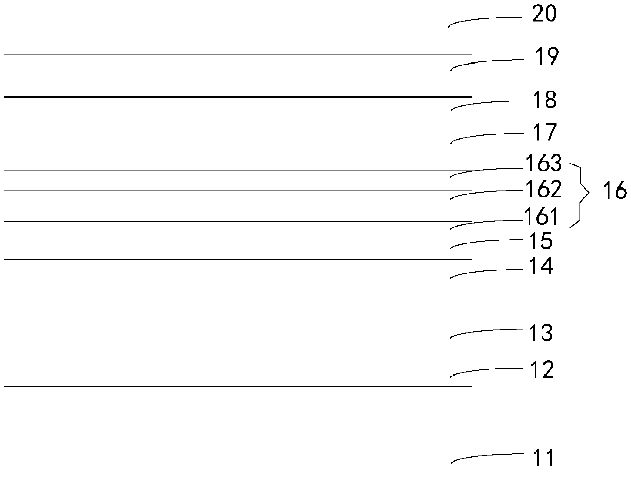
[0031] figure 1 It shows a GaN-based light-emitting diode epitaxial wafer provided by an embodiment of the present invention, see figure 1 , the epitaxial wafer includes: substrate 11, GaN buffer layer 12, GaN undoped layer 13, N-type doped GaN layer 14, shallow well layer 15, multiple quantum well layer 17, electron blocking layer 18, P-type GaN layer 19, and the P-type contact layer 20. The epitaxial wafer also includes a carrier blocking layer 16 located between the shallow well layer 15 and the multiple quantum well layer 17 . The carrier blocking layer 16 includes an AlInGaN layer 161 , an InGaN layer 162 , and an AlN layer 163 stacked in this order. The AlInGaN layer 161 is close to the shallow well layer 15 , and the AlN laye...


PUM

PropertyMeasurementUnit
Thicknessaaaaaaaaaa
Thicknessaaaaaaaaaa
Thicknessaaaaaaaaaa

Abstract

The invention discloses a GaN-based light emitting diode epitaxial wafer and a preparation method thereof and belongs to the technical field of a light emitting diode. The epitaxial wafer includes a substrate, a GaN buffer layer, a GaN non-doped layer, an N-type doped GaN layer, a shallow well layer, a multi-quantum well layer, an electron blocking layer, a P-type GaN layer and a P-type contact layer, the epitaxial wafer further includes a carrier blocking layer arranged between the shallow well layer and the multi-quantum well layer, wherein the carrier blocking layer include an AlInGaN layer, an InGaN layer and an AlN layer which are sequentially stacked, the AlInGaN layer is adjacent to the shallow well layer, and the AlN layer is adjacent to the multi-quantum well layer.

Description

technical field [0001] The invention relates to the technical field of light-emitting diodes, in particular to a GaN-based light-emitting diode epitaxial wafer and a preparation method thereof. Background technique [0002] GaN (Gallium Nitride) is a typical representative of the third-generation wide-bandgap semiconductor materials. It has excellent high thermal conductivity, high temperature resistance, acid and alkali resistance, and high hardness. It is widely used in the production of blue, green, and ultraviolet led. A GaN-based LED (Light Emitting Diode, light emitting diode) generally includes an epitaxial wafer and electrodes disposed on the epitaxial wafer. [0003] An existing GaN-based LED epitaxial wafer includes a substrate, a buffer layer, a GaN undoped layer, an N-type doped GaN layer, a shallow well layer, and a multi-quantum well layer ( Also known as active layer), electron blocking layer, P-type GaN layer, and P-type contact layer. When a current flows...

Claims


Application Information

Patent Timeline
IPC IPC(8): H01L33/06H01L33/14H01L33/00
CPCH01L33/007H01L33/06H01L33/145
Inventor 肖云飞唐成双刘春杨胡加辉李鹏
Owner HC SEMITEK ZHEJIANG CO LTD
Features
  • R&D
  • Intellectual Property
  • Life Sciences
  • Materials
  • Tech Scout
  • Unparalleled Data Quality
  • Higher Quality Content
  • 60% Fewer Hallucinations
Learn More