Foam-medium-based metamaterial with wide-band electromagnetic wave absorption

A foam material and metamaterial technology, applied in the field of foam dielectric-based metamaterials, can solve the problems of narrow frequency band and high density of wave absorbing materials, and achieve the effect of simple structure and good radar absorption performance.

Active Publication Date: 2019-03-29
INST OF METAL RESEARCH - CHINESE ACAD OF SCI
View PDF6 Cites 3 Cited by
  • Summary
  • Abstract
  • Description
  • Claims
  • Application Information

AI Technical Summary

Problems solved by technology

[0004] In order to solve the problems of narrow frequency band and high density of existing wave-absorbing materials, the purpose of the present invention is to provide a foam medium-based metamaterial for broadband electromagnetic wave absorption to achieve efficient broadband electromagnetic wave absorption

Method used


Image

  • Foam-medium-based metamaterial with wide-band electromagnetic wave absorption
  • Foam-medium-based metamaterial with wide-band electromagnetic wave absorption
  • Foam-medium-based metamaterial with wide-band electromagnetic wave absorption

Examples


Embodiment 1

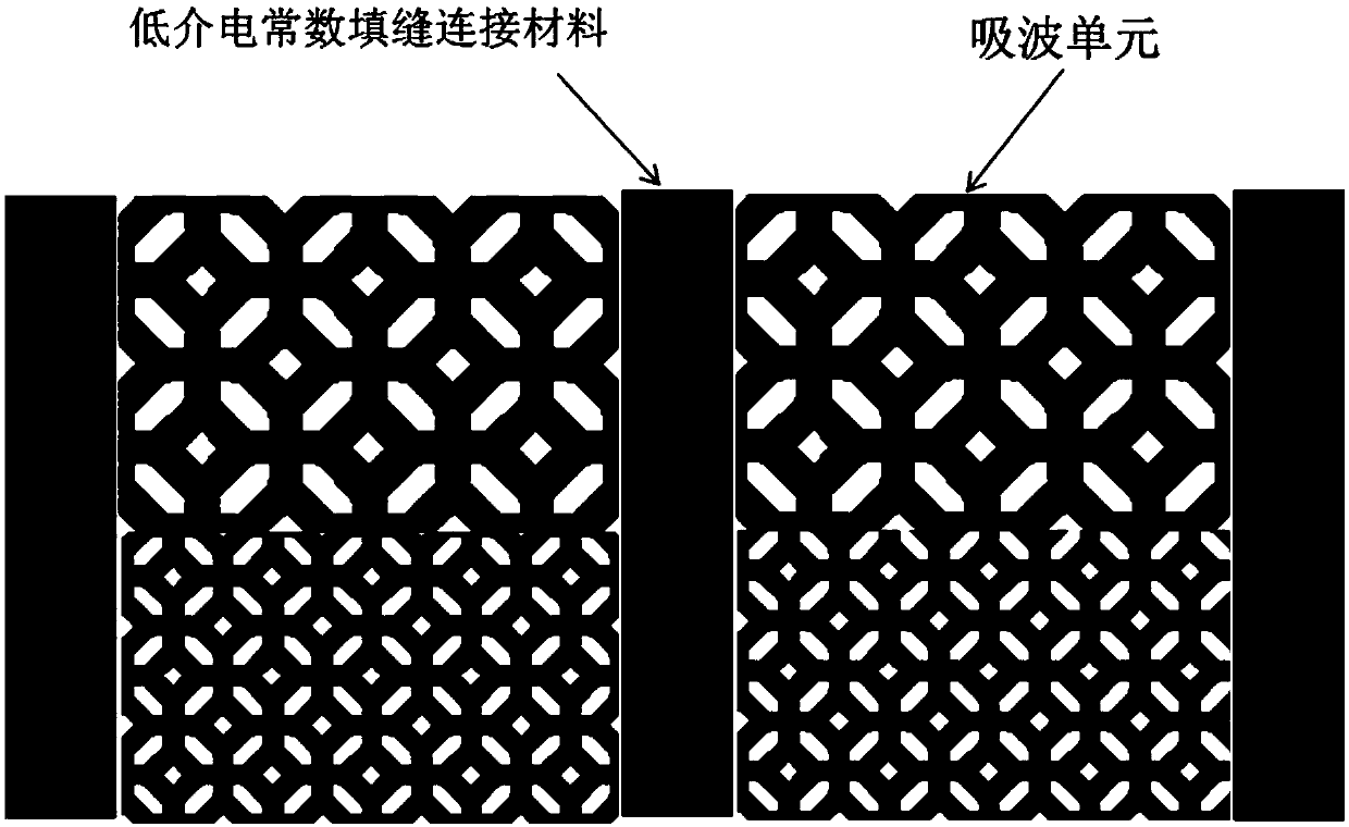
[0035] It consists of a material absorbing unit, and the combined material is carbon foam. Select a foam board with a mesh aperture of 1mm, an electrical conductivity of 0.7s / m-1s / m, and a thickness of 200mm, and process it into a square foam block of 20×20×6mm as the bottom layer material; Foam board with conductivity 0.6s / m, 200×200mm, plate thickness 20mm, processed into 20×20×4mm square foam block as the middle layer material; select mesh aperture 2mm, conductivity 0.2s / m, 200×200mm The foam board, with a thickness of 20mm, is processed into 20×20×4mm square foam pieces as the material for the incoming wave layer; several small pieces are bonded with a thin layer of epoxy resin less than 0.2mm, and each connected small piece The block is wrapped with a polyimide film with a thickness of 2 μm, and the foam block is glued to the bottom plate with epoxy resin, and the distance between the foam block is 3 mm, and put into the mold. The weight percentage is 88wt%: 2wt%: 10wt% ...

Embodiment 2

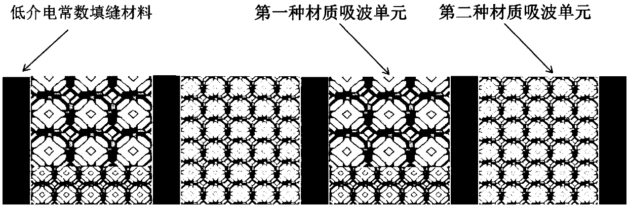
[0038] It is composed of a material absorbing unit, and the combined material is silicon carbide foam. Choose mesh aperture 4mm, resistivity 10 3 -10 10 Ω·m, 200×200mm foam board, 20mm thick; processed into 60×60×15mm square foam small pieces, each small piece is wrapped with a polyimide film with a thickness of 3μm, and the foam piece is covered with epoxy resin Stick to the bottom plate, the foam block spacing is 20mm, put into the mold. The weight percentage is 80wt%: 2wt%: 18wt% phenolic resin, p-toluenesulfonic acid and hollow glass microspheres with a particle size of 5-10 μm are mixed, and the mixture is filled in the gaps between the foams, and the mixture is combined with the above foam Completing hot-compression compounding in the mold, the compounding conditions are temperature control at 80°C and pressure at 8 MPa for 3 hours.

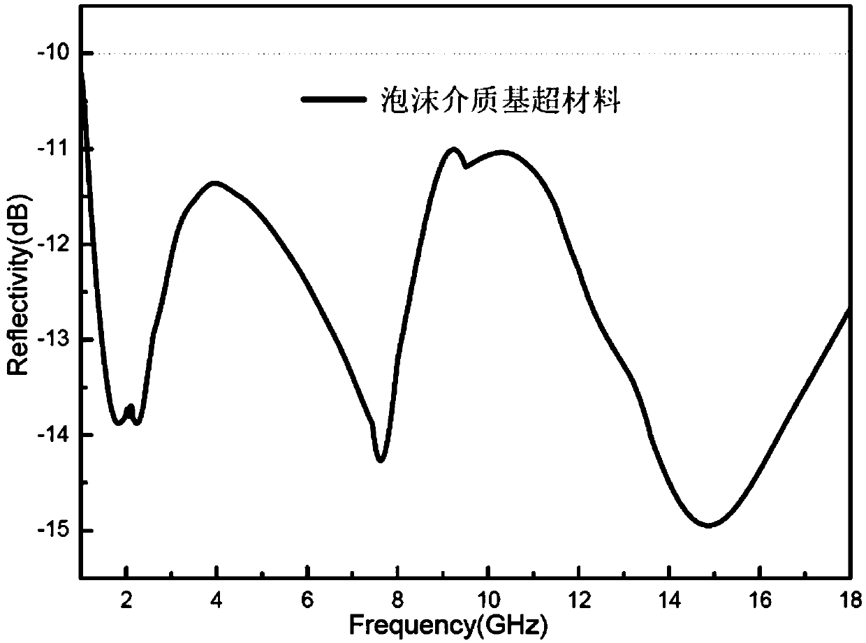
[0039] On the Agilent-N5230A network analyzer, the time domain test method is used to test the reflectivity of the flat panel. In this ...

Embodiment 3

[0041] It consists of a group of wave-absorbing units, and the combined material is foamed sendust. Select a foam board with a mesh aperture of 2 mm, a particle size of 80 μm, and a thickness of 200 mm, with a thickness of 20 mm; process it into a square foam block of 30 × 30 × 15 mm, and cover each small block with a polyimide film with a thickness of 5 μm For wrapping, glue the foam blocks to the bottom plate with epoxy resin, the distance between the foam blocks is 5mm, and put them into the mold. The weight percentage is 80wt%: 2wt%: 18wt% phenolic resin, p-toluenesulfonic acid and hollow glass microspheres with a particle size of 5-10 μm are mixed, and the mixture is filled in the gaps between the foams, and the mixture is combined with the above foam Completion of hot-compression lamination in the mold, the lamination conditions are temperature control 70 ℃, 7MPa pressure for 6 hours.

[0042] On the Agilent-N5230A network analyzer, the time domain test method is used t...


PUM

PropertyMeasurementUnit
pore sizeaaaaaaaaaa
electrical resistivityaaaaaaaaaa
particle diameteraaaaaaaaaa

Abstract

The invention, which belongs to the technical field of electromagnetic wave absorption, discloses a foam-medium-based metamaterial with wide-band electromagnetic wave absorption. The foam-medium-basedmetamaterial is formed by arranging a plurality of foam medium absorbing units on one same plane periodically. All foam medium absorbing units are connected into one through low-dielectric-constant joint filling materials, wherein the joint filling materials are prepared by mixing hollow glass microbeads, high polymer materials and curing agents and then carrying out solidifying and molding. Thefoam medium absorbing units are made of foamed silicon carbide, foamed carbon or iron-based foam materials. According to the foam-medium-based metamaterial, on the basis of advantages of lightweight,large scattering losses and interface polarization losses, and low impedance of foam materials, the maximum flat reflectance of the foam-medium-based metamaterial at the whole frequency range from 1 to 18 GHz is reduced to be below -10dB and the areal density is less than 9 kg / m<2> by fully utilizing the rich physical mechanisms of the metamaterial and the electromagnetic wave. The foam-medium-based metamaterial has the good broadband electromagnetic wave absorption performance.

Description

technical field [0001] The invention relates to the technical field of electromagnetic wave absorption, in particular to a foam medium-based metamaterial for broadband electromagnetic wave absorption. Background technique [0002] With the development of human technology, electromagnetic waves are used more and more widely in daily life. Electromagnetic waves are involved in aircraft navigation, mobile communication, wireless networks, etc. Electromagnetic waves interfere with each other and even electromagnetic wave pollution becomes increasingly prominent; in the military field, with With the improvement of radar detection technology, the ability of electromagnetic stealth and camouflage also needs to be strengthened. Therefore, developing and preparing high-efficiency absorbing materials has become a key issue in the field of materials. [0003] Traditional absorbing materials have been greatly restricted in application due to factors such as narrow bandwidth and high su...

Claims


Application Information

Patent Timeline
Patent Type & Authority Applications(China)
IPC IPC(8): H01Q17/00
CPCH01Q17/008
Inventor 张劲松李万崇李处森林立海
Owner INST OF METAL RESEARCH - CHINESE ACAD OF SCI
Why Eureka
Try Eureka