

High-precision detection method for the concentration and distribution of trace impurity elements in Gan
A detection method and technology for trace impurities, which are applied in the direction of material analysis, measurement device, and material analysis using wave/particle radiation, which can solve the problems of low detection accuracy, incomplete types of impurity elements, and inability to distinguish the types of impurity elements.
- Summary
- Abstract
- Description
- Claims
- Application Information
AI Technical Summary
Problems solved by technology
Method used
Image

Examples
Embodiment Construction
[0034] Specific embodiments of the present invention will be described in detail below in conjunction with specific drawings. It should be noted that the technical features or combinations of technical features described in the following embodiments should not be regarded as isolated, and they can be combined with each other to achieve better technical effects. In the drawings of the following embodiments, the same reference numerals appearing in each drawing represent the same features or components, which can be applied in different embodiments.
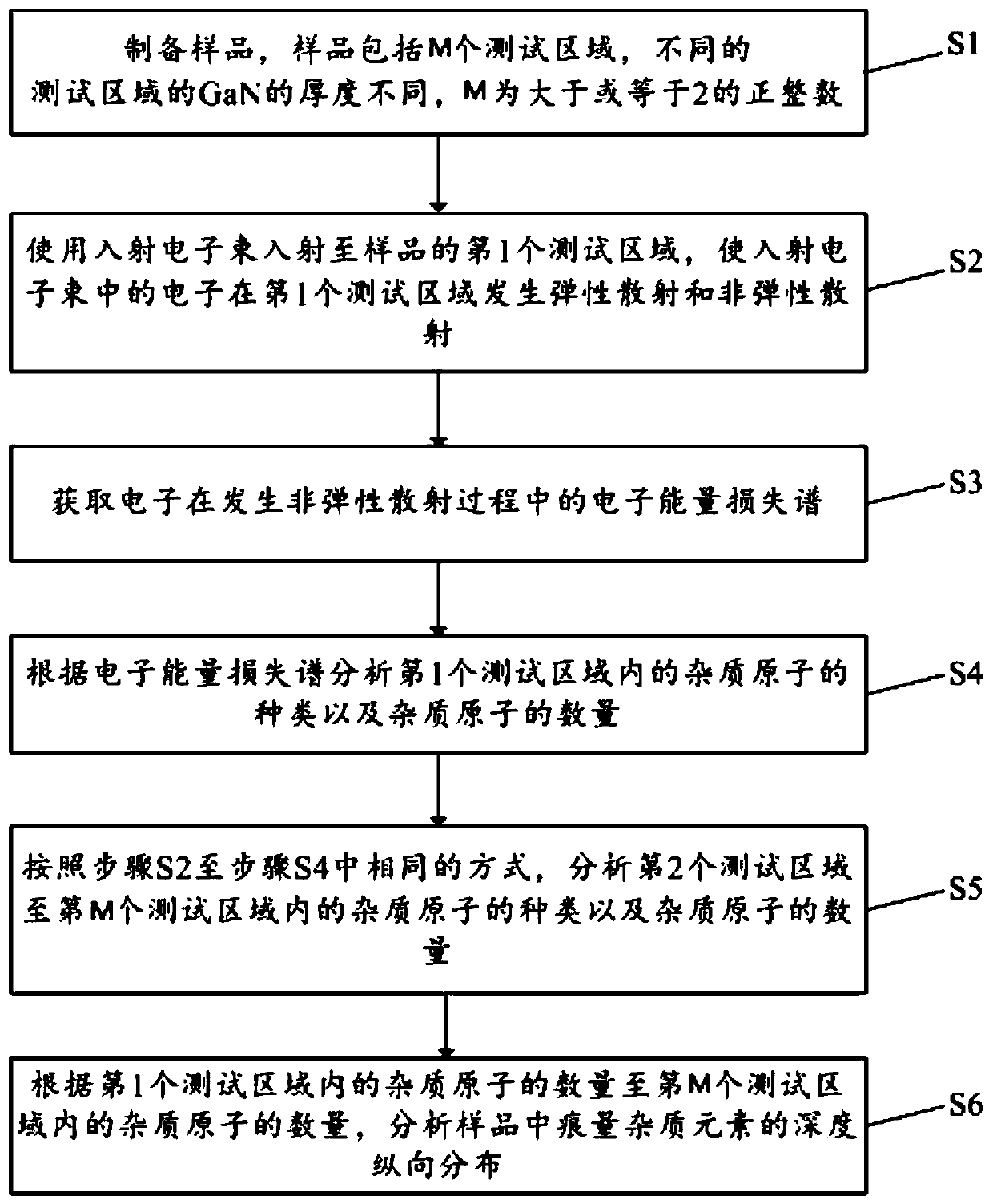
[0035] An embodiment of the present invention is a high-precision detection method for the concentration and distribution of trace impurity elements in GaN (hereinafter referred to as a high-precision detection method), specifically, as figure 1 as shown, figure 1 A schematic flow chart of a high-precision detection method provided by an embodiment of the present invention, the high-precision detection method includes:
[0036] S...
PUM
 Abstract
Description
Claims
Application Information