Thick-copper copper substrate etching process
A copper substrate and process technology, applied in the field of PCB production, can solve the problems of poor precision, high hole processing cost, and inability to process special-shaped through holes, etc., to achieve the effect of reducing processing cost, improving production efficiency and production quality
- Summary
- Abstract
- Description
- Claims
- Application Information
AI Technical Summary
Problems solved by technology
Method used
Image


Examples
Embodiment Construction
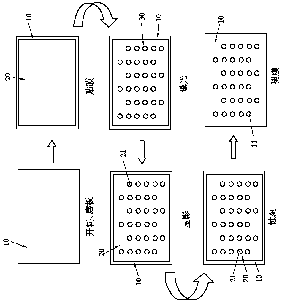
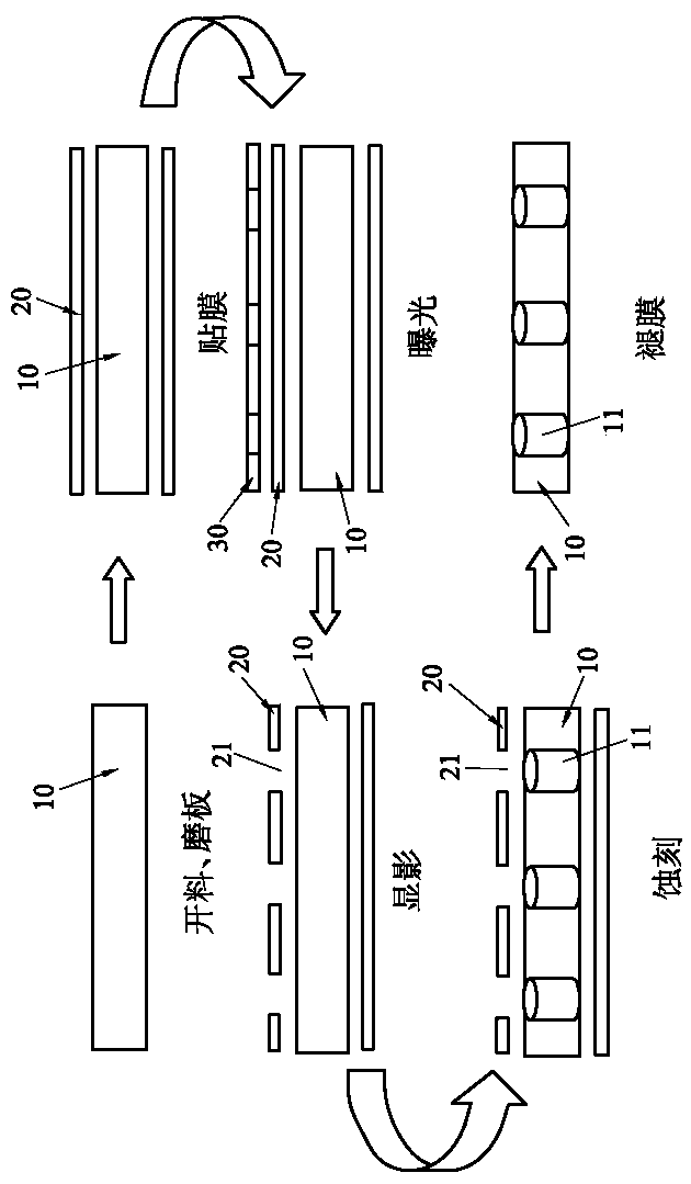
[0024] The invention discloses a pitting process for a thick copper copper substrate, which includes the following steps:
[0025] (1) Cutting: Cut thick copper and copper substrates to 10 sizes according to product requirements.
[0026] (2) Grinding: Grinding the thick copper-copper substrate 10 to appropriately increase the roughness of the surface of the thick copper-copper substrate 10 while cleaning the surface. In this embodiment, during the grinding process, the size of the wear scar is controlled to be 12-16mm, the mass concentration of pozzolan used is 15-25%, the temperature is controlled at 80-90°C, and the speed is controlled at 2.0-2.5m / min.
[0027] (3) Film sticking: sticking resist ink or dry film 20 on the surface of the thick copper-copper substrate 10 . In this embodiment, the film sticking is carried out at a temperature of 110-130° C., and the speed is controlled at 1.2-1.4 m / min.
[0028] (4) Exposure: the image is transferred to the resist ink or dry ...
PUM
 Abstract
Description
Claims
Application Information
 - R&D
- Intellectual Property
- Life Sciences
- Materials
- Tech Scout
- Unparalleled Data Quality
- Higher Quality Content
- 60% Fewer Hallucinations
Browse by: Latest US Patents, China's latest patents, Technical Efficacy Thesaurus, Application Domain, Technology Topic, Popular Technical Reports.
© 2025 PatSnap. All rights reserved.Legal|Privacy policy|Modern Slavery Act Transparency Statement|Sitemap|About US| Contact US: help@patsnap.com