Method for controllably preparing composite nano pattern array

A composite and array technology, which is used in the coupling of optical waveguides, the fabrication of microstructure devices, and the process for producing decorative surface effects. and other problems, to achieve the effect of simple and controllable spacing, less interference of organic components, and diversified substrate morphology and configuration.

Active Publication Date: 2019-04-09
CHONGQING BIO NEWVISION MEDICAL EQUIP LTD
View PDF12 Cites 15 Cited by
  • Summary
  • Abstract
  • Description
  • Claims
  • Application Information

AI Technical Summary

Problems solved by technology

[0007] The present invention provides a method for overcoming the defects of cumbersome construction steps, low order and density, long preparation period, high cost and harsh test conditions in the prior art. Simple, high order and high density, short preparation period, low price and simple test conditions, a controllable method for preparing composite nanopattern arrays

Method used


Image

  • Method for controllably preparing composite nano pattern array
  • Method for controllably preparing composite nano pattern array

Examples


Embodiment 1

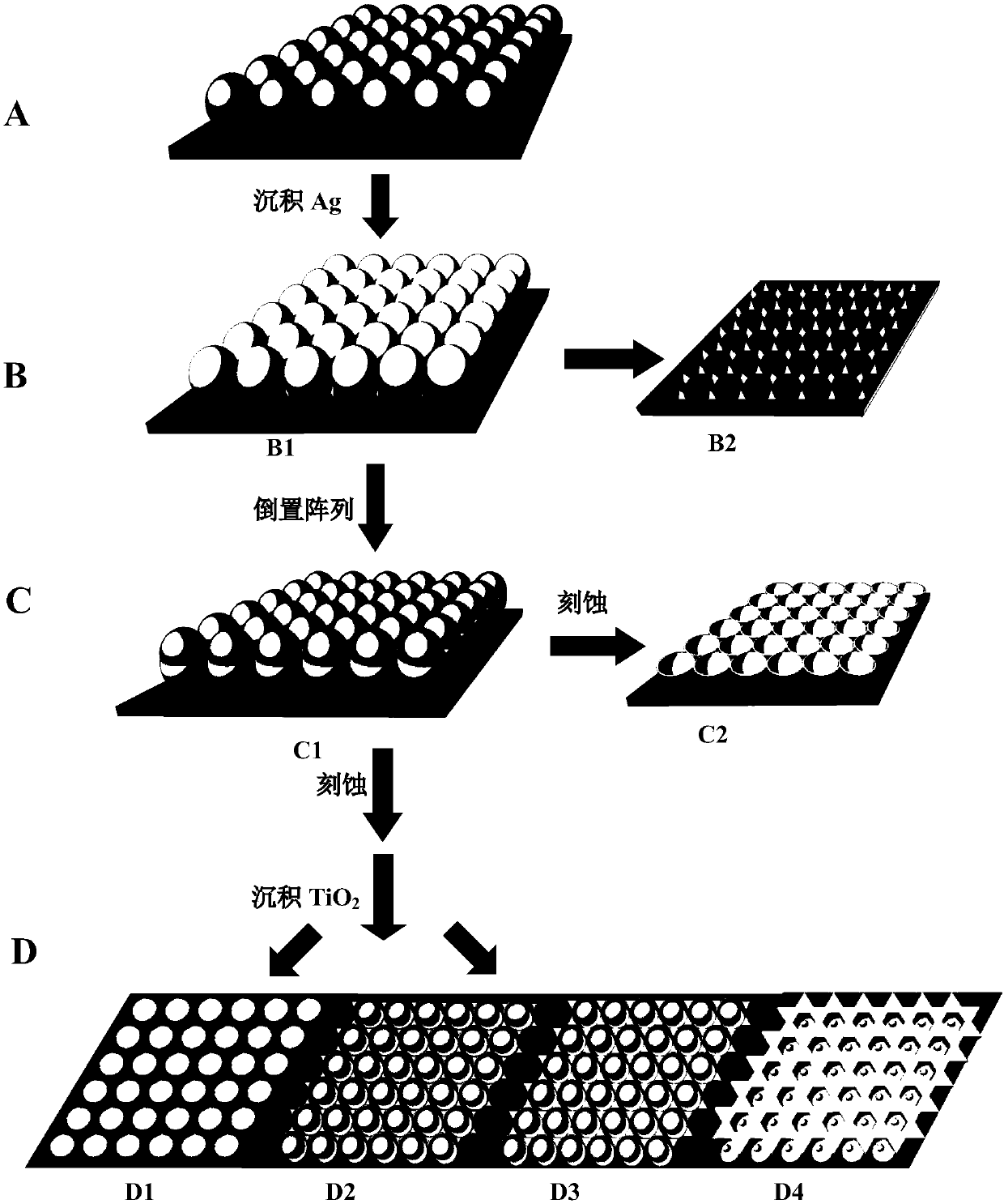
[0032] Such as figure 1 As shown, a controllable method for preparing composite nanopattern arrays, the preparation method includes the following steps:

[0033] (A) Using the self-assembly method, a densely packed array of PS colloidal balls with a diameter of 200 nm was self-assembled on a Si substrate with a hydrophilic surface to obtain an ordered nano-patterned structural template;

[0034] (B) After magnetron sputtering a layer of Ag film with a thickness of 20nm on the surface of the ordered nanopatterned structure template obtained in step (A), an Ag nanocap array (as shown in B1) is formed; the surface is coated with Ag The PS colloidal ball array of the film is glued down with double-sided adhesive, and the Ag nanotriangular array is obtained on the original Si substrate (as shown in B2);

[0035] (C) Transfer the double-sided adhesive with the PS colloidal ball array with Ag film on the surface in step (B) upside down to another Si substrate, and re-expose the PS t...

Embodiment 2

[0038] The difference from Example 1 is that in this example, the etching time in step (D) is changed to 60s, and a layer of TiO with a thickness of 50nm is deposited on the surface by sputtering 2 Ag-TiO 2 Nanocap-star array (shown in D2).

Embodiment 3

[0040] The difference from Example 1 is that in this example, the etching time in step (D) is changed to 120s, and a layer of TiO with a thickness of 50nm is deposited on the surface by sputtering 2 Ag-TiO 2 Nanocap-star array (shown in D3).


PUM

PropertyMeasurementUnit
diameteraaaaaaaaaa
thicknessaaaaaaaaaa
diameteraaaaaaaaaa

Abstract

The invention belongs to the technical field of nano composite material synthesis, and particularly relates to a method for controllably preparing a composite nano pattern array. The method comprisesthe steps: sputtering an Ag film on the surface of an ordered nano patterned structure template to form an Ag nano cap array and an Ag nano triangular array; inversely transferring the Ag nano cap array to another Si substrate to obtain a secondary template; completely etching PS spheres to obtain an Ag nano-bowl array; etching the PS spheres for different time periods, and sputtering and depositing a TiO2 film on the surface of each PS sphere to obtain an Ag-TiO2-FON array, an Ag-TiO2 nanocap-Star array and an Ag-TiO2 nanoring-particle array. According to the invention, the defects of tediousconstruction steps, low orderliness and density, long preparation period, high cost, rigorous test condition requirements and the like of the ordered nanostructure active substrate in the prior art are overcome, so that the method has the advantages of good uniformity, high orderliness, high repeatability, simple construction steps, short preparation period and low cost.

Description

technical field [0001] The invention belongs to the technical field of synthesis of nanocomposite materials, and in particular relates to a method for controllably preparing composite nanopattern arrays. Background technique [0002] When a light wave (electromagnetic wave) is incident on the interface between the metal and the medium, the free electrons on the metal surface are driven by the light wave electromagnetic field to oscillate collectively, forming a near-field electromagnetic wave that propagates along the metal surface, which is surface plasmon or surface etc. From polaritons (Surface Plasmons, SPs). Surface plasmons have a series of novel optical properties, such as selective absorption and scattering of light, local electric field enhancement, subwavelength confinement of electromagnetic waves, and so on. The surface plasmons excited on the interface between the metal film and the medium can propagate along the film to form conductive surface plasmons (surfac...

Claims


Application Information

Patent Timeline
Patent Type & Authority Applications(China)
IPC IPC(8): B81B7/04B81C1/00
CPCB81B7/04B81C1/00031
Inventor 温嘉红赵晓宇王雅新张永军
Owner CHONGQING BIO NEWVISION MEDICAL EQUIP LTD
Why Eureka
Try Eureka