Semiconductor packaging mould, semiconductor device and packaging method of semiconductor device
A packaging method and semiconductor technology, applied in semiconductor devices, semiconductor/solid-state device parts, semiconductor/solid-state device manufacturing, etc., can solve problems such as peeling of packaging materials and chips, and warping of packaging materials or chips. Small, the effect of reducing the possibility of peeling
- Summary
- Abstract
- Description
- Claims
- Application Information
AI Technical Summary
Problems solved by technology
Method used
Image

Examples
no. 1 example
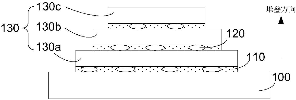
[0051] Please refer to figure 1 , a plurality of chips 130 are stacked on the packaging substrate 100.
[0052] The packaging substrate 100 functions to support and protect the chip 130 . The material of the packaging substrate 100 includes, but is not limited to: epoxy resin, polyimide, and the like. Specifically, in the embodiment of the present invention, the material of the packaging substrate 100 is epoxy resin.
[0053] The shape of the chip 130 is square, circular, etc., and there is no specific limitation here. Specifically, in the embodiment of the present invention, the shape of the chip 130 is square. The base material of chip 130 is silicon.
[0054] Each chip 130 includes opposite first and second surfaces. Specifically, in the embodiment of the present invention, the first surface refers to the top surface of each chip 130 , and the second surface refers to the bottom surface of each chip 130 .
[0055] It should be noted that there is no specific limitati...
no. 2 example
[0089] The difference between the second embodiment and the first embodiment lies in that the outline shape of the chip receiving cavity of the packaging mold is different, and the other parts and the positional relationship between the parts are consistent with the first embodiment.
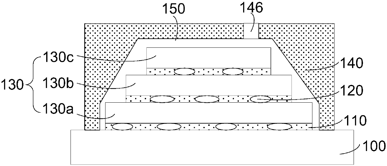
[0090] Please refer to Figure 5 , cover the stacked chips 230 with the packaging mold 240 .
[0091] Functions and positional relationships of the packaging substrate 200 , the metal interconnection structure 210 , and the filling material 220 are consistent with those of the first embodiment, and will not be repeated here.
[0092] Please refer to the first embodiment for the shape, stacking method, positional relationship, and width dimension of the chips 230 .
[0093] The encapsulation mold 240 covers the stacked chips 230 for subsequent filling of encapsulation material. The chip receiving cavity accommodates all the chips 230 , and the profile of the chip receiving cavity of the packagi...
no. 3 example
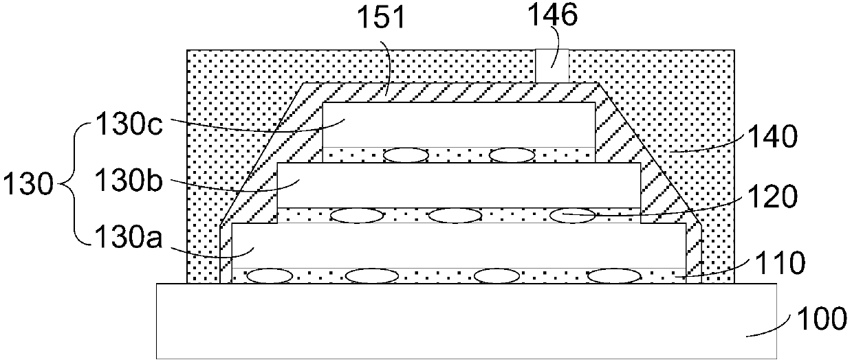
[0120] The difference between the third embodiment and the second embodiment lies in the outline shape of the chip containing cavity of the packaging mold and the stacking manner of the chips. One side of the cross-sectional profile shape of the packaging mold chip accommodation cavity in the depth direction is a plane, and at the same time, one side of all the stacked chips is kept flush. For the functions and positional relationships of other components of the third embodiment, please refer to the second embodiment.
[0121] Please refer to Figure 9 , a plurality of chips 330 are stacked on the packaging substrate 300 .
[0122] The functions and materials of the packaging substrate 300 are consistent with those of the second embodiment, and will not be repeated here.
[0123] Chips 330 are stacked on the package substrate 300 . The functions of stacking the chips 330 , the connection methods between different chips 330 and between the chips 330 and the package substrate...
PUM
 Abstract
Description
Claims
Application Information
 - R&D
- Intellectual Property
- Life Sciences
- Materials
- Tech Scout
- Unparalleled Data Quality
- Higher Quality Content
- 60% Fewer Hallucinations
Browse by: Latest US Patents, China's latest patents, Technical Efficacy Thesaurus, Application Domain, Technology Topic, Popular Technical Reports.
© 2025 PatSnap. All rights reserved.Legal|Privacy policy|Modern Slavery Act Transparency Statement|Sitemap|About US| Contact US: help@patsnap.com