Power semiconductor module and packaging method thereof

A technology of power semiconductors and chips, which is applied in the direction of semiconductor devices, semiconductor/solid-state device manufacturing, semiconductor/solid-state device components, etc., can solve problems such as high voltage spikes and complex matching processes, so as to alleviate voltage spikes and reduce design difficulty Effect

Active Publication Date: 2020-12-15
JILIN SINO MICROELECTRONICS CO LTD +1
View PDF4 Cites 0 Cited by
  • Summary
  • Abstract
  • Description
  • Claims
  • Application Information

AI Technical Summary

Problems solved by technology

In the improved scheme of CN 101290927 B "Circuit Device with Freewheeling Diode", the high-voltage high-frequency oscillation problem of the reverse recovery of the SiC Schottky barrier diode is improved, but the reverse recovery characteristic is still determined by the silicon PiN diode. When the di / dt in the circuit is very high and the conduction pulse width or continuous current is small, high voltage spikes will still occur
At the same time, SiC Schottky barrier diodes, silicon PiN diodes, and switch tube IGBT switch control require a very complicated matching process

Method used


Image

  • Power semiconductor module and packaging method thereof
  • Power semiconductor module and packaging method thereof
  • Power semiconductor module and packaging method thereof

Examples


Embodiment 1

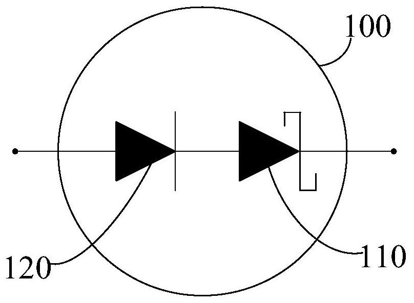
[0043] An embodiment of the present invention provides a power semiconductor module, which uses a damping module to replace the fast recovery diode connected in parallel with the switch chip, such as figure 1 As shown, the damping module 100 includes:

[0044] The voltage blocking chip 110 and the damping chip 120 are connected in series.

[0045] The voltage blocking chip 110 has fast recovery characteristics and low soft characteristics, and may be a Schottky barrier diode, or an ultrafast recovery diode with low junction capacitance.

[0046] The reverse withstand voltage value of the voltage blocking chip 110 satisfies the following formula:

[0047]

[0048] in, is the reverse withstand voltage value of the voltage blocking chip, L S is the circuit stray inductance or transformer leakage inductance flowing through the voltage blocking chip, is the rate of change of current in the circuit flowing through the voltage blocking chip.

[0049] The damping chip 120 is ...

Embodiment 2

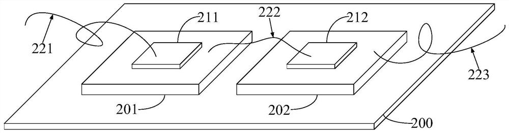
[0057] In the power semiconductor module provided by the embodiment of the present invention, the principle of the damping module is the same as that of the first embodiment, the difference is that the structure diagram of the damping module is different, such as Figure 4 As shown, the damping module includes: ceramic base copper clad board (abbreviated as DCB board)-400, copper clad module-401, voltage blocking chip-411, damping chip 412, wire 421, wire 422.

[0058] Among them, the DCB board 400 only includes a copper-clad module 401, the diode cathode in the voltage blocking chip 411 and the diode anode in the damping chip 412 are welded together by welding, and the diode cathode in the damping chip 412 is welded to the copper-clad module. , forming a parallel package.

[0059] The packaged damping module is connected in parallel with the switch chip in the power semiconductor module through the wire 421 and the wire 422, replacing the fast recovery diode in the traditiona...

Embodiment 3

[0062] This embodiment provides a packaging method for power semiconductor modules, which is applied to damping modules, such as Figure 5 shown, including the following steps:

[0063] S510: setting a first copper clad area and a second copper clad area on the DCB board.

[0064] The DCB board is a ceramic-based copper-clad laminate, which means that the copper foil is directly bonded to the alumina (Al 2 o 3 ) or aluminum nitride (AlN) ceramic substrate surface, in this step, two copper clad areas are set on the DCB board for carrying the voltage blocking chip and the damping chip contained in the damping module.

[0065] S520: welding the voltage blocking chip to the first copper-clad area, and welding the damping chip to the second copper-clad area.

[0066] The voltage blocking chip and the damping chip in the damping module are connected to their respective copper clad areas through soldering pieces, wherein the negative pole of the voltage blocking chip is connected ...


PUM


Abstract

The invention provides a power semiconductor module and a packaging method thereof and relates to the technical field of power semiconductor module development. The power semiconductor module comprises a damping module, wherein the damping module comprises a voltage blocking chip and a damping chip which are packaged together; and the negative electrode of the voltage blocking chip is connected with the positive electrode of the damping chip. Through the power semiconductor module provided by the invention, a fast recovery diode, which is in parallel with a switch chip, in a conventional powersemiconductor module can be replaced by the damping module, thereby alleviating the voltage spike generated in the reverse recovery process and reducing the design difficulty of a switch chip driver.

Description

technical field [0001] The invention relates to the technical field of power semiconductor module development, in particular to a power semiconductor module and a packaging method thereof. Background technique [0002] Power semiconductor modules are widely used in chopper or inverter circuits, mainly including controllable switching devices and freewheeling devices. The turn-on and turn-off speed of the switching device in the power semiconductor module directly affects the power loss of the module, and at the same time restricts the operating frequency of the power module. Affecting the switching speed of the power module is not only the inherent speed factor of the switching device itself, but also the stray inductance and leakage inductance in the circuit, and the parasitic capacitance of the freewheeling chip and other devices. In the high-voltage, high-current application environment, the stray inductance and leakage inductance current in the circuit will generate hig...

Claims


Application Information

Patent Timeline
Patent Type & Authority Patents(China)
IPC IPC(8): H01L23/31H01L23/488H01L21/56H01L21/60
CPCH01L21/56H01L23/3114H01L23/488H01L24/03H01L2224/48091H01L2924/00014
Inventor 左义忠杨寿国高宏伟邢文超
Owner JILIN SINO MICROELECTRONICS CO LTD
Why Eureka
Try Eureka