High-efficiency heterojunction battery intrinsic amorphous silicon passivation layer structure and preparation method thereof
A technology of intrinsic amorphous silicon and heterojunction cells, applied in circuits, photovoltaic power generation, electrical components, etc., can solve problems such as microvoid defects, solar cell performance deterioration, etc., to avoid epitaxial growth, enhance interface passivation, The effect of increasing the hydrogen content of the film
- Summary
- Abstract
- Description
- Claims
- Application Information
AI Technical Summary
Problems solved by technology
Method used
Image

Examples
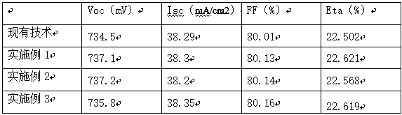
Embodiment 1
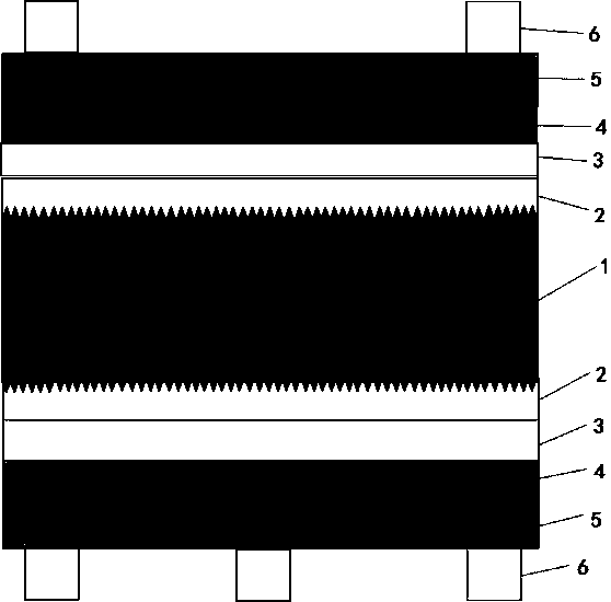
[0031] see figure 1 , the present invention relates to an intrinsic amorphous silicon passivation layer structure for a high-efficiency heterojunction battery, which includes an N-type crystalline silicon wafer 1, and the front and back sides of the N-type crystalline silicon wafer 1 are provided with two layers of amorphous Silicon intrinsic layer 2, that is, the first amorphous silicon intrinsic layer 2 and the second amorphous silicon intrinsic layer 3;
[0032] The thickness of the first intrinsic layer 2 of amorphous silicon is 4nm, and the intrinsic layer 2 of the first amorphous silicon adopts the PECVD method. 2 Depositing, that is, using pure silane to deposit; the thickness of the second amorphous silicon intrinsic layer 3 is 4nm, and the second amorphous silicon intrinsic layer 3 is made of H 2 Diluted S i h 4 are deposited, the H 2 :S i h 4 1:1;
[0033] The first layer of amorphous silicon intrinsic layer 2 uses pure silane to prevent epitaxial growth and H...
Embodiment 2
[0047] see figure 1 , the present invention relates to an intrinsic amorphous silicon passivation layer structure for a high-efficiency heterojunction battery, which includes an N-type crystalline silicon wafer 1, and the front and back sides of the N-type crystalline silicon wafer 1 are provided with two layers of amorphous Silicon intrinsic layer 2, that is, the first amorphous silicon intrinsic layer 2 and the second amorphous silicon intrinsic layer 3;
[0048] The thickness of the first intrinsic layer 2 of amorphous silicon is 3 nm, and the intrinsic layer 2 of the first amorphous silicon cannot pass H through PECVD. 2 Deposition, that is, using pure silane for deposition; the thickness of the second amorphous silicon intrinsic layer 3 is 5nm, and the second amorphous silicon intrinsic layer 3 is made of H 2 Diluted S i h 4 are deposited, the H 2 :S i h 4 2:1;
[0049] The first layer of amorphous silicon intrinsic layer 2 uses pure silane to prevent epitaxial gro...
Embodiment 3
[0063] see figure 1 , an intrinsic amorphous silicon passivation layer structure for a high-efficiency heterojunction battery that the present invention involves, it includes an N-type crystalline silicon wafer 1, and the front and back sides of the N-type crystalline silicon wafer 1 are provided with three layers of amorphous silicon Intrinsic layer 2, that is, the first intrinsic layer of amorphous silicon 2, the second intrinsic layer of amorphous silicon 3 and the third intrinsic layer of amorphous silicon;
[0064] The thickness of the first intrinsic layer 2 of amorphous silicon is 3 nm, and the intrinsic layer 2 of the first amorphous silicon cannot pass H through PECVD. 2 Deposition, that is, depositing by pure silane; the thickness of the second amorphous silicon intrinsic layer 3 is 3nm, and the second amorphous silicon intrinsic layer 3 is made of H 2 Diluted S i h 4 For deposition, the H of the second amorphous silicon intrinsic layer 3 2 :S i h 4 1:1; the th...
PUM
| Property | Measurement | Unit |
|---|---|---|
| thickness | aaaaa | aaaaa |
| thickness | aaaaa | aaaaa |
| thickness | aaaaa | aaaaa |
Abstract
Description
Claims
Application Information