LED chip structure of ITO structure and preparing method thereof
A technology of LED chip and multi-quantum well structure, which is applied in the direction of electrical components, circuits, semiconductor devices, etc., can solve the problems of P-GaN lateral expansion difficulty, large effective light emitting area of the chip, etc. Optical, high conductivity effect
- Summary
- Abstract
- Description
- Claims
- Application Information
AI Technical Summary
Problems solved by technology
Method used
Image
Examples
Embodiment 1
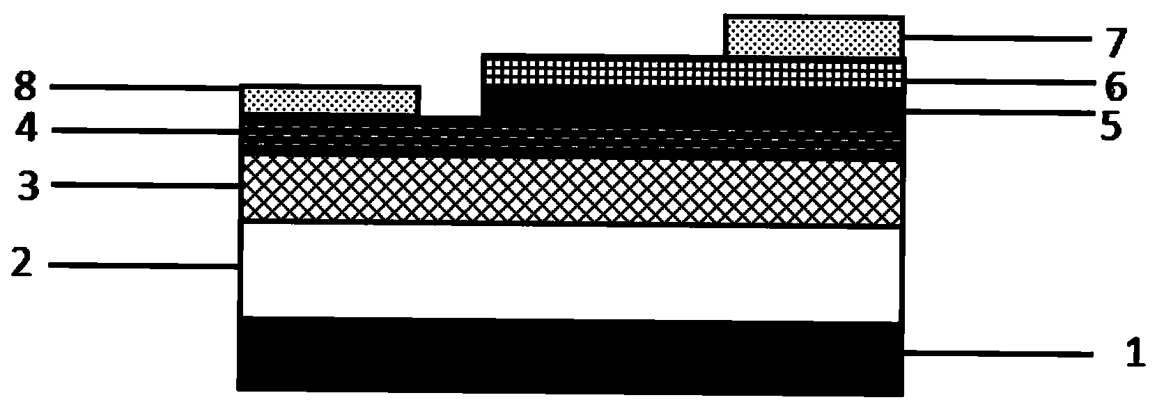
[0031] See attached figure 1 Shown, a kind of ITO structure LED chip structure and preparation method thereof, comprises the following steps:
[0032] 1) Using MOCVD or MBE to grow a nucleation layer 2 on the substrate 1, the growth temperature is 520-570°C, and the thickness is 10-30nm;
[0033] 2) growing a U-GaN layer 3 on the nucleation layer 2 at a growth temperature of 1080° C. and a thickness of 2-4 μm, which is an unintentional undoped layer;
[0034] 3) growing an N-GaN layer 4 on the U-GaN layer 3 at a growth temperature of 1080° C., a thickness of 0.2-1 μm, and Si doping at a concentration of 5E17 to 3E18;
[0035] 4) On the N-GaN layer 4, grow the InGaN / GaN multi-quantum well layer 5 for about 5-10 cycles, wherein the growth temperature is 650-850°C for the InGaN layer, 700-900°C for the GaN layer, and the In composition is 10%, and finally The growth cut-off layer is a GaN layer;
[0036] 5) pickling the surface of the epitaxial wafer;
[0037] 6) Carrying out...
PUM
 Abstract
Description
Claims
Application Information
