LED chip structure of graphene structure and manufacturing method thereof

A graphene and graphene layer technology, applied in electrical components, circuits, semiconductor devices, etc., can solve the problems of large effective light emitting area of ​​the chip and difficulty in lateral expansion of P-GaN, and achieve the relief of metal electrode blocking area and high light transmission. The effect of high conductivity and high conductivity

Inactive Publication Date: 2015-01-21
华芯半导体科技有限公司
View PDF4 Cites 7 Cited by
  • Summary
  • Abstract
  • Description
  • Claims
  • Application Information

AI Technical Summary

Problems solved by technology

[0006] The present invention utilizes the high electrical conductivity and high light transmittance of the graphene material, which can effectively alleviate the problems that

Method used


Image

  • LED chip structure of graphene structure and manufacturing method thereof

Examples


Embodiment 1

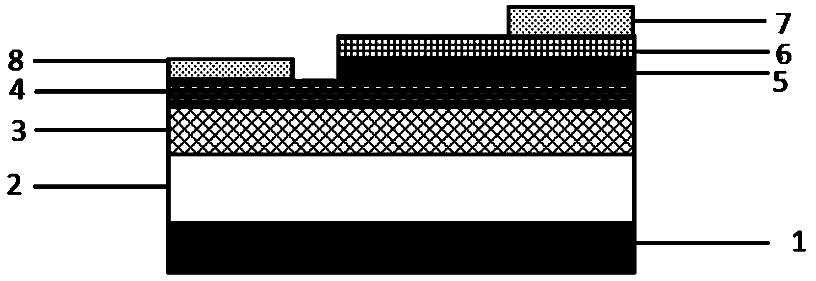
[0042] Embodiment one: see attached figure 1 Shown, a kind of graphene LED chip structure and preparation method thereof, comprises the following steps:

[0043] 1) Using MOCVD or MBE to grow a nucleation layer 2 on the substrate 1, the growth temperature is 520-570°C, and the thickness is 10-30nm;

[0044] 2) growing a U-GaN layer 3 on the nucleation layer 2 at a growth temperature of 1080° C. and a thickness of 2-4 μm without doping;

[0045] 3) growing an N-GaN layer 4 on the U-GaN layer 3 at a growth temperature of 1080° C., a thickness of 0.2-1 μm, and a Si doping concentration of 5E17˜3E18;

[0046]4) On the N-GaN layer 4, grow the InGaN / GaN multi-quantum well layer 5 for about 5-10 periods, wherein the growth temperature is 650-850° C. for the InGaN layer, with a thickness of 1-5 nm, and 700-900° C. for the GaN layer, with a thickness of 5-5 nm. 10nm, In composition is 10%, and the final growth cut-off layer is GaN layer;

[0047] 5) pickling the surface of the epita...


PUM


Abstract

The invention discloses an LED chip structure of a graphene structure and a manufacturing method of the LED chip structure. A nucleating layer, a non-doped GaN layer, an N-type doped GaN layer and an InGaN/GaN multiple-quantum-well structure are formed on a substrate in an epitaxial mode; after the multiple-quantum-well structure grows in the epitaxial mode, growth is stopped, and a P-type doped graphene layer is adopted for replacing a P-type GaN epitaxial layer; a P electrode is manufactured on the P-type doped graphene layer, the N-type doped GaN layer is formed through etching and an N electrode is manufactured on the N-type doped GaN layer; the P electrode is correspondingly arranged on the P-type doped graphene layer; an epitaxial wafer is etched, and the N electrode is manufactured on the N-type doped GaN layer. Through the LED chip structure of the graphene structure and the manufacturing method of the LED chip structure, maldistribution of In groups caused by P-GaN growing after the InGaN/GaN multiple-quantum-well structure through temperature rise can be avoided, and wavelength homogeneity can be improved easily; epitaxial growth of the P-GaN is avoided, cost is reduced, and productivity is improved; an ultrathin graphene layer high in light transmission and conductivity is adopted as a P-type current expanding layer, the light outgoing efficiency can be effectively improved, and the external quantum efficiency can be improved.

Description

technical field [0001] The invention relates to a graphene-structured LED chip structure and a preparation method thereof, belonging to the technical field of semiconductor epitaxy and chips. Background technique [0002] With the development of modern industry, the global energy crisis and air pollution problems have become increasingly prominent. LED has the advantages of high light efficiency, low power consumption, long life, high safety, high environmental protection, etc. It is an ideal lighting method, and more and more countries pay attention to it. [0003] Incandescent lamps and tungsten-halogen lighting effects are 12-24 lumens / watt, fluorescent lamps are 50-70 lumens / watt, and sodium lamps are 90-140 lumens / watt. Most of the power consumption becomes heat loss. After the LED light effect is improved, it will reach 50-200 lumens / watt, and its monochromaticity is good, the spectrum is narrow, and it can directly emit colored visible light without filtering. The d...

Claims


Application Information

Patent Timeline
IPC IPC(8): H01L33/06H01L33/26
CPCH01L33/06H01L33/0075H01L33/26H01L2933/0008
Inventor 王智勇张杨杨翠柏杨光辉
Owner 华芯半导体科技有限公司
Why Eureka
Try Eureka