

Susceptor designs for silicon carbide thin films
A base and equipment technology, applied in gaseous chemical plating, chemical instruments and methods, from chemically reactive gases, etc., can solve problems such as uneven doping levels and shortened base life
- Summary
- Abstract
- Description
- Claims
- Application Information
AI Technical Summary
Problems solved by technology
Method used
Image

Examples
Embodiment Construction
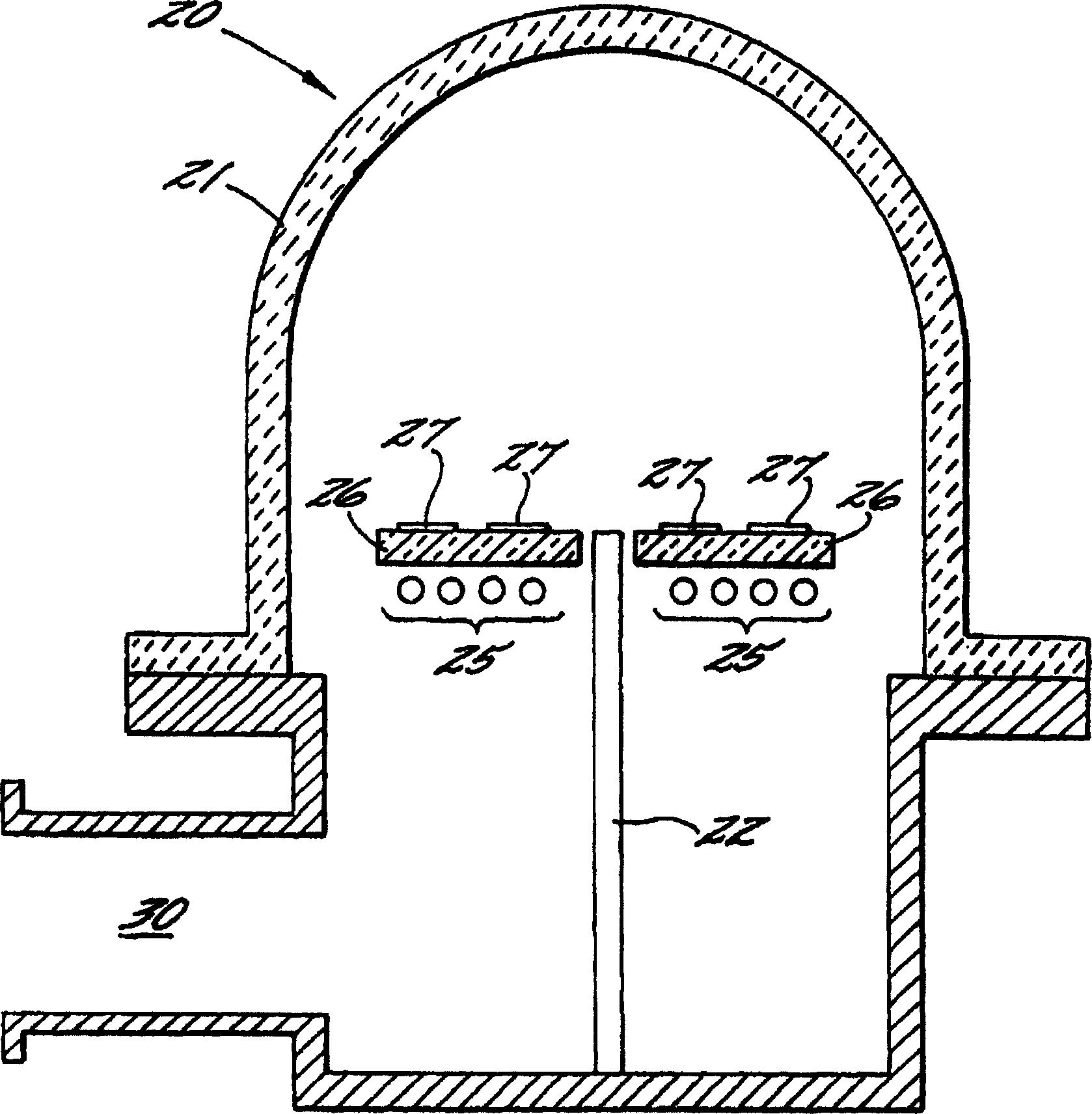
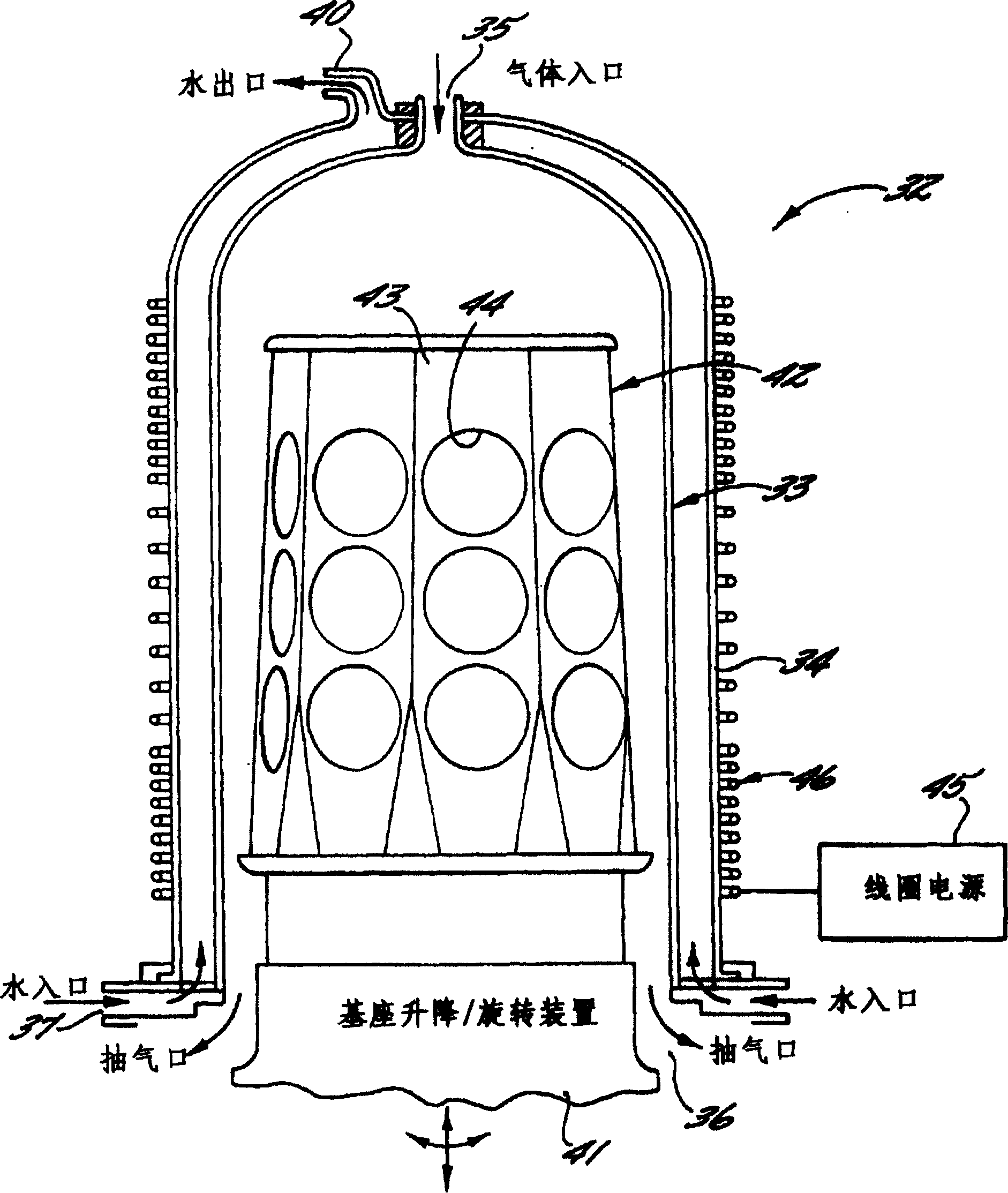
[0030]The present invention is a susceptor for minimizing or eliminating temperature gradients including radial, axial and surface-to-surface gradients affecting a substrate wafer during epitaxial growth. Substrate pair according to the invention figure 1 with 2 The chemical vapor deposition system shown is particularly useful. figure 1 A platform or flat CVD system, generally indicated at 20, is shown. The system comprises a reaction vessel 21, ie bell jar, generally made of quartz tubing material which is substantially transparent to electromagnetic radiation of the appropriate frequency. The gas supply system is in fluid communication with the reaction vessel 21, and at figure 1 is shown as a gas injector 22 .
[0031] This system includes a source of electromagnetic radiation, in figure 1 is shown as induction coil 25 . The operation of such generators and induction coils is well known to those of ordinary skill in the art and therefore will not be discussed in m...
PUM
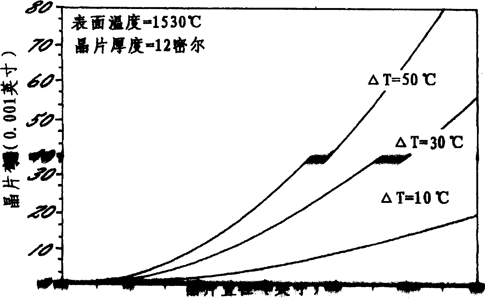
| Property | Measurement | Unit |
|---|---|---|
| surface temperature | aaaaa | aaaaa |
Abstract
Description
Claims
Application Information