Ultra-wideband absorber based on combined resonant structure, and manufacturing method thereof

A resonant structure and ultra-wideband technology, which is applied in the field of ultra-wideband absorbers and their manufacturing, can solve the problems of increased device thickness, high construction time and cost, and increased design difficulty, so as to reduce thickness, time and cost Effect

Inactive Publication Date: 2019-04-19
INNER MONGOLIA UNIVERSITY
View PDF3 Cites 9 Cited by
  • Summary
  • Abstract
  • Description
  • Claims
  • Application Information

AI Technical Summary

Problems solved by technology

[0004] In view of the existing technical problems, the present invention provides an ultra-broadband absorber based on a combined resonant structure and its manufacturing method, which solves the problem of the sublattice structure contained in the metamaterial unit structure of the existing absorber. It is impossible to increase the number indefinitely, and the multilayer stacked metamaterial structure will lead to an increase in the thickness of the device, and its construction time and cost are high, and the design difficulty will increase sharply as the frequency increases

Method used


Image

  • Ultra-wideband absorber based on combined resonant structure, and manufacturing method thereof
  • Ultra-wideband absorber based on combined resonant structure, and manufacturing method thereof
  • Ultra-wideband absorber based on combined resonant structure, and manufacturing method thereof

Examples


Embodiment 1

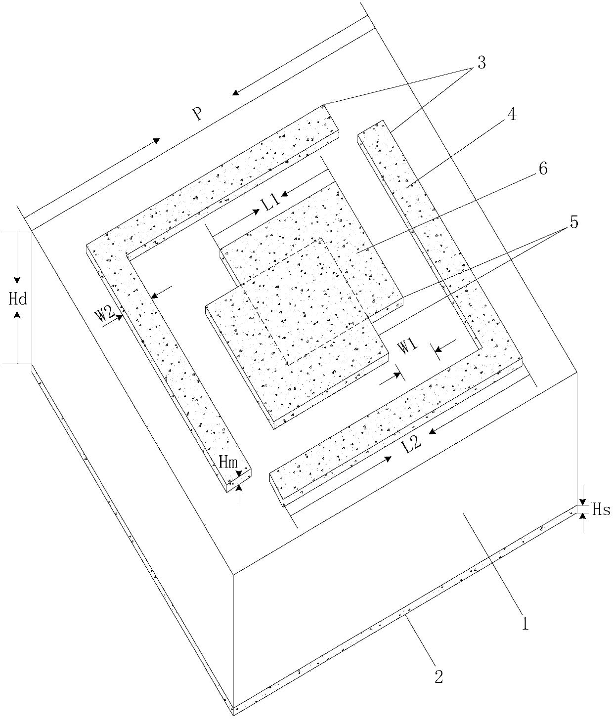
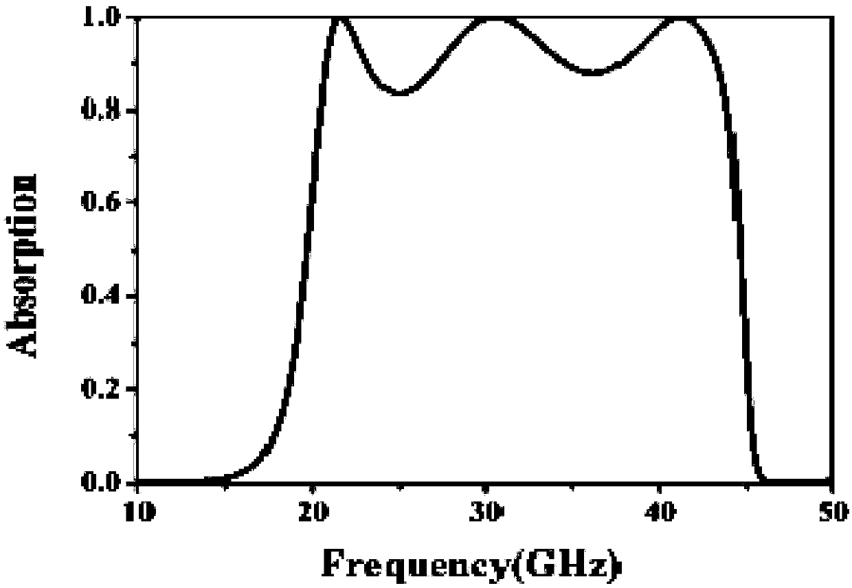
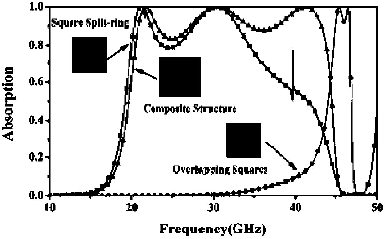
[0035] see figure 1 , this embodiment provides an ultra-broadband metamaterial absorber based on a combined resonant structure, which is used to solve many obstacles encountered in bandwidth expansion methods such as the common planar structure method and multi-layer stacking method, especially in the structural In the process of ultra-wideband metamaterial absorber, the above two methods no longer have the problem of obtaining the prerequisites for ultra-wideband absorbing. Among them, the ultra-wideband metamaterial absorber based on the combined resonant structure of this embodiment includes a dielectric layer 1, a thin film 2, a first resonant structure 3 and a second resonant structure 5, which can be applied to stealth devices (such as weapons such as stealth fighters) equipment) or solar cells.

[0036] The dielectric layer 1 has two end surfaces that are far away from each other. In this embodiment, the shape of the two end surfaces of the dielectric layer 1 is prefer...

Embodiment 2

[0049] This embodiment provides a method for manufacturing an ultra-broadband metamaterial absorber based on a combined resonant structure, which can be used to manufacture the absorber in Example 1, and includes the following steps:

[0050] (1) According to the shape of the film 2, the positioning groove is first excavated on the base material, and then the coating is started from the bottom of the positioning groove to achieve a film 2 with a preset thickness of 1; wherein, the depth of the positioning groove is not less than the dielectric layer 1 , the sum of the thicknesses of the thin film 2 and the first resonant structure 3;

[0051] (2) After the film 2 is shaped, a liquid medium material is poured into the positioning groove to form a medium layer 1 with a preset thickness of 2;

[0052] (3) After the dielectric layer 1 is shaped, a resonant material is placed on the dielectric layer 1 to form a resonant film with a preset thickness of 1, and the resonant film is et...

Embodiment 3

[0055] This embodiment provides a wave-absorbing patch, which includes a patch and a plurality of wave-absorbing components uniformly arranged on the same surface of the patch. Wherein, the patch can be made of flexible material so as to be pasted on various structures, and the wave absorber in the embodiment 1 is used as the absorber, and the film 2 is fixed on the other side of the patch. It should be noted here that the wave-absorbing sticker provided in this embodiment can be applied as a whole product. The wave-absorbing sticker provided in this embodiment can be pasted on the surface or inside of various devices to absorb electromagnetic waves, it can be pasted on various military equipment in the military field, and it can also be pasted on electronic products to prevent electromagnetic interference.


PUM


Abstract

The invention discloses an ultra-wideband absorber based on a combined resonant structure, and a manufacturing method thereof. The ultra-wideband absorber includes a dielectric layer, a film, a firstresonant structure and a second resonant structure, wherein the dielectric layer is provided with two end faces away from each other; the film is laid on one end surface of the dielectric layer; the first resonant structure is mounted on the other end surface of the dielectric layer and includes two first resonant units disposed opposite to each other; the first resonant units are L-shaped, and anopening ring structure is formed through enclosure of the two first resonant units; the second resonant structure is mounted on the other end face of the dielectric layer and is located in the opening ring structure; the second resonant structure includes two second resonant units each in a square shape; and the two second resonant units are partially overlapped. The ultra-wideband absorber basedon a combined resonant structure enables the waveforms absorbed by the first resonant structure and the second resonant structure to be linearly superimposed to form an absorbing band having a plurality of harmonic absorption peaks, thus breaking the constraint of the original two bandwidth expansion methods, and reducing the time and the cost of device construction.

Description

technical field [0001] The invention relates to a wave absorber in the technical field of wave absorption, in particular to an ultra-wideband wave absorber based on a combined resonant structure and a manufacturing method thereof. Background technique [0002] Microwave absorbers usually have a small physical size and can have specific absorption capabilities in the target frequency domain. In recent years, they have been widely used in various civil and military fields such as preventing electromagnetic interference and electromagnetic stealth. In the military field, microwave absorbers can be used as coatings for weapons and equipment, so that weapons have the ability of electromagnetic stealth, and the opponent cannot detect our personnel through weapons. RCS for various flying units. The application of microwave absorbers in specific life is mainly reflected in the microwave absorbing applications that most electronic products need to prevent electromagnetic interferenc...

Claims


Application Information

Patent Timeline
Patent Type & Authority Applications(China)
IPC IPC(8): H01Q17/00H05K9/00
CPCH01Q17/008H05K9/006
Inventor 王鑫王俊林翁智韩丁
Owner INNER MONGOLIA UNIVERSITY
Why Eureka
Try Eureka