

Multi-line cutting method, multi-line cutting device and application thereof, semiconductor material and power device
A multi-wire cutting and cutting-line technology, which is applied in the fields of semiconductor materials and power devices, multi-wire cutting methods and multi-wire cutting devices, can solve the problems of difficult processing of semiconductor substrates, achieve small warpage and increase energy , The effect of enhancing the cutting ability
Active Publication Date: 2019-04-23
FUJIAN NORSTEL MATERIAL TECH CO LTD
View PDF7 Cites 1 Cited by
- Summary
- Abstract
- Description
- Claims
- Application Information
AI Technical Summary
Problems solved by technology
At present, in the manufacture and epitaxial growth of next-generation power devices, there are strict requirements on the final surface quality of substrate materials. However, due to the high hardness of the above-mentioned semiconductor materials (such as the Mohs hardness of SiC crystal is 9.2, second diamond), the chemical stability is very good (almost no obvious chemical reaction with other substances at room temperature), so the semiconductor substrate is difficult to process
Method used
View moreImage
Smart ImageViewing Examples

Examples
Embodiment 1
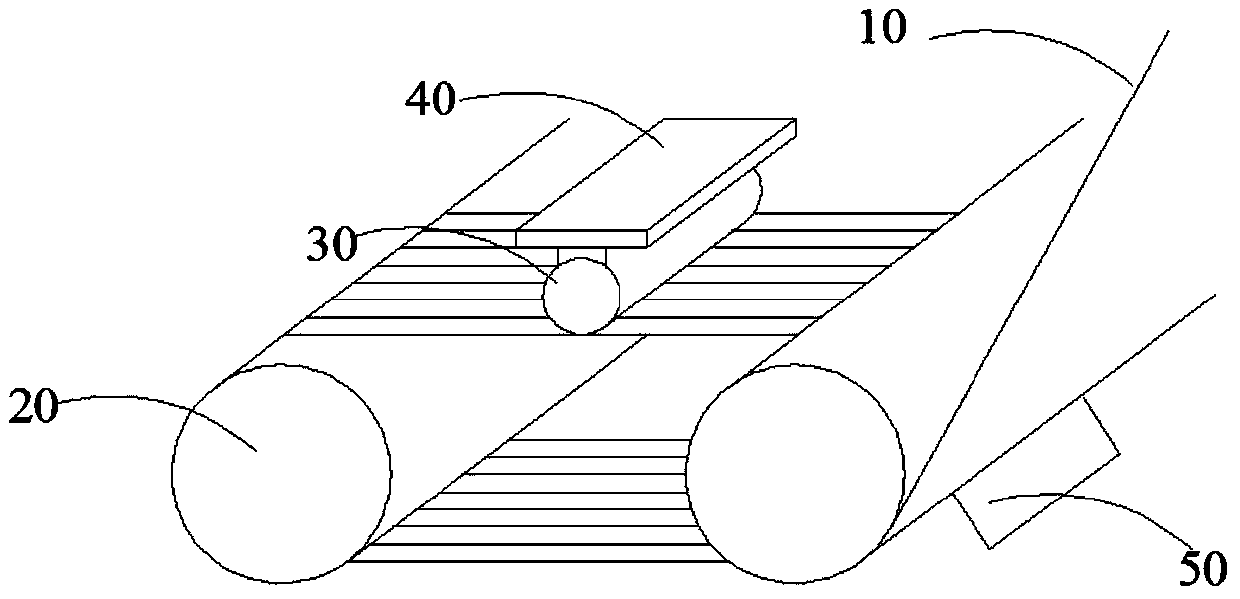
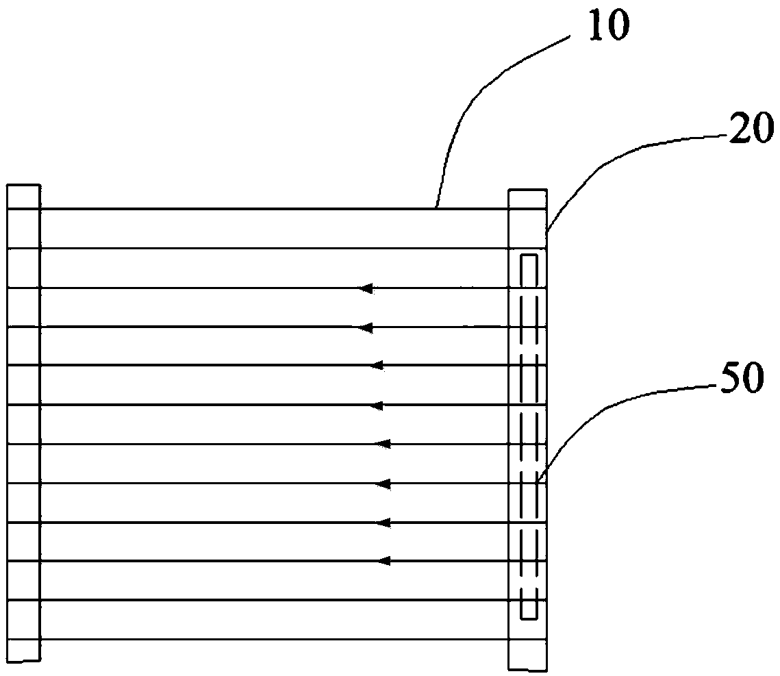
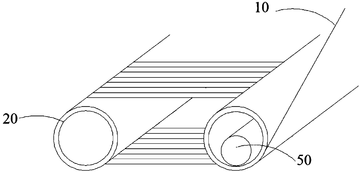
[0066] Multi-wire cutting methods include:
[0067] The spool is in contact with the vibrating head of the ultrasonic generator, and the spool vibrates under the excitation of ultrasonic waves with a frequency of 20kHz. Under the transmission of the spool, the cutting line vibrates and the object to be cut is cut. The diameter of the cutting line is 0.2mm , The moving speed of the cutting line is 500 m / min.
Embodiment 2
[0069] The multi-wire cutting method is the same as in Example 1, except that the frequency of the ultrasonic wave is 300 kHz.
Embodiment 3
[0071] The multi-wire cutting method is the same as in Example 1, except that the frequency of the ultrasonic wave is 150kHz.
Login to View More PUM
| Property | Measurement | Unit |
|---|---|---|
| diameter | aaaaa | aaaaa |
| tension | aaaaa | aaaaa |
| Resonant frequency | aaaaa | aaaaa |
Abstract
The invention provides a multi-line cutting method, a multi-line cutting device and application thereof, a semiconductor material and a power device, and relates to the technical field of multi-line cutting. The multi-line cutting method comprises the following steps that a line spool for winding cutting lines vibrates under the excitation action of ultrasonic waves, and the cutting lines vibrateand cut a to-be-cut object under the conveying action of the line spool. The cutting line vibrate under the excitation action of the ultrasonic waves, energy of the cutting lines can be increased, thecutting capability of the cutting lines can be enhanced, abrasion of the cutting lines can be reduced, abrasive materials can be forced to impact and grind the to-be-cut object at the high frequencyand speed, the chip removal speed is high, therefore, the surface curvature, the surface warpage and the total thickness deviation of a product obtained after cutting are all small, and the cutting quality is high.
Description
Technical field [0001] The present invention relates to the technical field of multi-wire cutting, in particular to a multi-wire cutting method, a multi-wire cutting device and its use, semiconductor materials and power devices. Background technique [0002] The third-generation wide-bandgap semiconductor materials (such as single crystal silicon carbide) have excellent performance. In recent years, they have rapidly penetrated into the fields of lighting, power devices, microwave and radio frequency, etc., and have the ability to manufacture high-frequency and high-power devices that are resistant to high temperature and radiation. The broad application prospects have become the focus of international attention. At present, in the manufacturing and epitaxial growth of next-generation power devices, there are strict requirements on the final surface quality of the substrate material. However, due to the high hardness of the above-mentioned semiconductor materials (for example, th...
Claims
Login to View More Application Information
Patent Timeline
 Patent Type & AuthorityApplications(China)
IPC IPC(8): B28D5/04B28D7/00
CPCB28D5/0058B28D5/045B28D5/047B28D5/0082
Inventor赖柏帆张洁林武庆
OwnerFUJIAN NORSTEL MATERIAL TECH CO LTD