Workpiece processing methods and process chambers

A processing method and technology of a process chamber, which are applied to the processing of workpieces and the field of process chambers of workpieces, can solve the problems of increased production cost, easy falling of particles, small roughness value, etc., so as to reduce production cost and reduce particle impurities. , The effect of improving the processing yield

Active Publication Date: 2021-12-17
BEIJING NAURA MICROELECTRONICS EQUIP CO LTD
View PDF11 Cites 0 Cited by
  • Summary
  • Abstract
  • Description
  • Claims
  • Application Information

AI Technical Summary

Problems solved by technology

Obviously, this will greatly prolong the return time of the machine and increase the production cost
Secondly, in the daily production process, due to the small roughness value of the lower surface of the media window, the adsorption of particles is insufficient, which causes the particles on the lower surface of the media window to fall and cause the problem of unqualified particles on the machine
[0007] Additionally, if image 3 As shown, in traditional etching equipment, the existing focus ring is mostly made of quartz, which is generally processed by machining + HF (hydrofluoric acid) soaking for 60 minutes, and the contact part with the wafer is processed with a higher The roughness value is Ra1.6, and the roughness value of the rest is Ra3.2, which is relatively rough
In actual use, the focus ring is closer to the wafer, the roughness value of its upper surface is larger, and the adsorption force for process by-products is stronger. Therefore, some process by-products can be deposited on the surface of the focus ring, thereby forming new The source of particles, this part of the particles are easy to fall to the surface of the wafer, causing process defects to the wafer

Method used


Image

  • Workpiece processing methods and process chambers
  • Workpiece processing methods and process chambers
  • Workpiece processing methods and process chambers

Examples


Embodiment Construction

[0056]Specific embodiments of the present invention will be described in detail below in conjunction with the accompanying drawings. It should be understood that the specific embodiments described here are only used to illustrate and explain the present invention, and are not intended to limit the present invention.

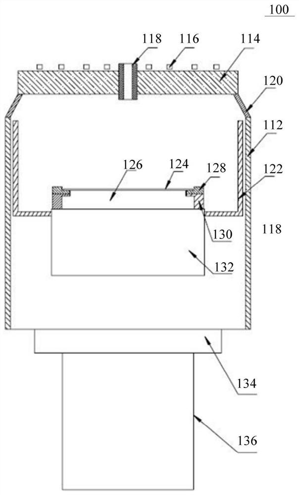
[0057] Such as Figure 4 As shown, the first aspect of the present invention relates to a processing method S100 of a workpiece, the workpiece is placed in a process chamber.

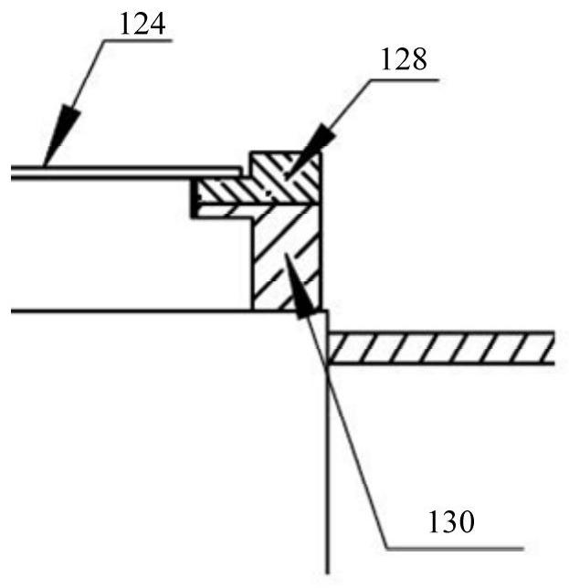
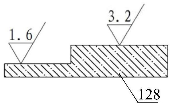
[0058] It should be noted that although the specific type of workpiece is not clearly limited. However, as pointed out in the background technology, in a traditional process chamber, the focus ring surrounding the wafer and the dielectric window at the top of the process chamber opposite to the wafer, these two parts have a significant impact on the wafer. The processing yield has a great influence. Therefore, the present invention mainly provides a processing method for the two parts, ...


PUM


Abstract

The invention discloses a workpiece processing method and a process chamber. The method includes: providing a blank of the workpiece; performing rough processing on the blank to obtain a preliminary semi-finished product; finishing processing the surface of the preliminary semi-finished product to obtain an intermediate semi-finished product, wherein the surface roughness value of the intermediate semi-finished product is Ra 1 <1.6: Predetermined treatment is performed on the surface of the intermediate semi-finished product to obtain the workpiece, wherein the surface roughness value of the workpiece conforms to a preset roughness value. In the process chamber structure of the workpiece formed by applying the processing method of the workpiece, it can effectively reduce the particle impurities generated on the surface of the wafer, improve the processing yield of the wafer, reduce the production cost, and improve the economic benefit.

Description

technical field [0001] The invention relates to the technical field of semiconductor manufacturing, in particular to a processing method for a workpiece and a process chamber including the workpiece manufactured by the processing method. Background technique [0002] When the traditional etching machine is etching the wafer, once the process by-products land on the surface of the wafer, it will form particulate impurities, resulting in poor etching process. Therefore, in order to ensure the etching yield of the wafer, the particle impurities in the process need to be strictly controlled. [0003] Such as figure 1 with figure 2 Shown is a schematic diagram of the structure of the etching machine. Wherein, the etching machine 100 includes a reaction chamber 112, a dielectric window 114 located at the top of the reaction chamber, a radio frequency coil 116, a nozzle 118, an adjustment bracket 120 located between the reaction chamber 112 and the dielectric window 114, and is...

Claims


Application Information

Patent Timeline
Patent Type & Authority Patents(China)
IPC IPC(8): H01J37/32
CPCH01J37/32642H01J37/32871
Inventor 黄亚辉李一成刘建曹永友
Owner BEIJING NAURA MICROELECTRONICS EQUIP CO LTD
Why Eureka
Try Eureka