Preparation method of semiconductor nano material

A nanomaterial and semiconductor technology, which is applied in the field of semiconductor nanomaterial preparation, can solve the problems of wide size distribution of one-dimensional semiconductor nanocrystals, cumbersome preparation methods, and large particles of impurities, and achieve small size distribution, high electron mobility, and The effect of high purity

Inactive Publication Date: 2021-07-16
TCL CORPORATION
View PDF2 Cites 0 Cited by
  • Summary
  • Abstract
  • Description
  • Claims
  • Application Information

AI Technical Summary

Problems solved by technology

At present, researchers have tried a variety of methods to prepare one-dimensional semiconductor nanocrystals, such as template method, solvothermal method, electrodeposition method, etc. However, the existing preparation methods are relatively cumbersome, and the obtained one-dimensional semiconductor nanocrystals have a wide size distribution. , large particles with many impurities and low purity

Method used


Image

  • Preparation method of semiconductor nano material
  • Preparation method of semiconductor nano material

Examples


preparation example Construction

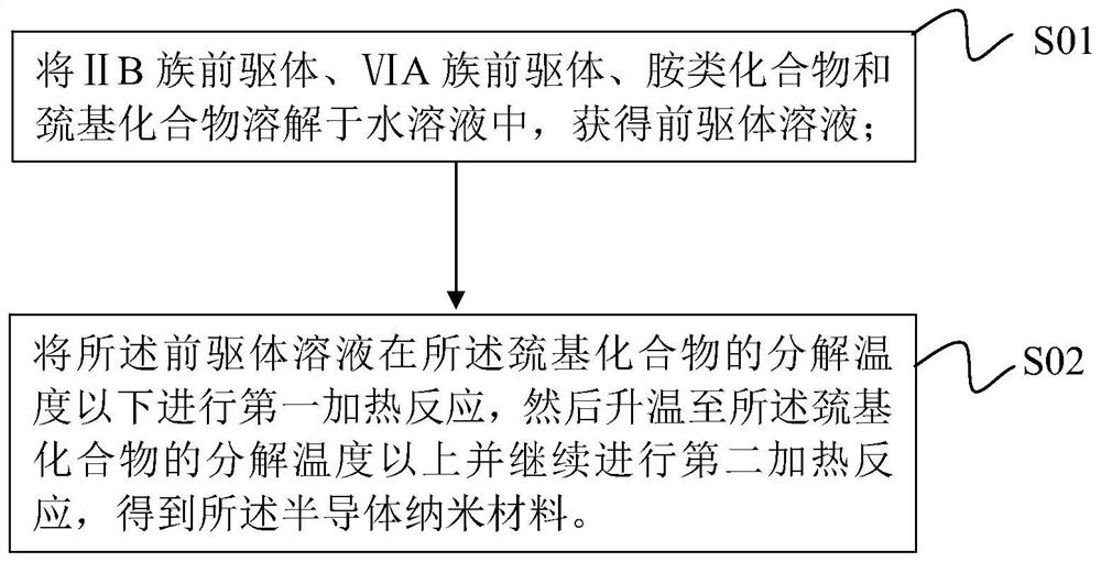
[0019] A method for preparing semiconductor nanomaterials, such as figure 1 shown, including the following steps:

[0020] S01, dissolving the Group IIB precursor, the Group VIA precursor, the amine compound and the mercapto compound in an aqueous solution to obtain a precursor solution;

[0021] S02. Perform a first heating reaction on the precursor solution below the decomposition temperature of the mercapto compound, then raise the temperature to above the decomposition temperature of the mercapto compound and continue the second heating reaction to obtain the semiconductor nanomaterial.

[0022] In the method for preparing semiconductor nanomaterials provided in the embodiments of the present invention, the precursor solution in which group IIB precursors, group VIA precursors, amine compounds, and mercapto compounds are dissolved is sequentially subjected to a first heating reaction and a second heating reaction, and By adjusting and controlling the reaction temperature ...

Embodiment approach

[0027] In the embodiment of the present invention, the amine compound is used as a structure inducer to induce the synthesis of a one-dimensional semiconductor nanomaterial. In the synthesis process of one-dimensional semiconductor nanomaterials, the amine compounds tend to coordinate with the empty orbitals of the IIB group cations located in the peripheral direction of the crystal, which to a certain extent inhibits the combination of the IIB group cations in the crystal peripheral direction and the selenium anion, making The combination rate of group IIB cations in the crystal axial direction and selenium anions is greater than that in the crystal peripheral direction, and then forms semiconductor nanomaterials in the form of nanorods or nanowires. As an embodiment, the amine compound includes at least one of ethylenediamine, ethylenediamine diacetic acid and ethylenediamine diacetate, and this type of amine compound can be linearly coordinated with Cd and Zn atoms, Promote...

Embodiment 1

[0056] This embodiment provides a semiconductor nanomaterial, the preparation of which specifically includes the following steps:

[0057] (1) Add 10mmol of zinc chloride, 3mmol of thioglycolic acid, 20mmol of ethylenediaminetetraacetic acid, and 500mmol of deionized water into a 50mL three-necked flask, and stir at 1000rpm under Ar atmosphere protection until dissolved at room temperature to obtain the first mixed solution.

[0058] 5 mmol of selenium, 10 mmol of sodium borohydride, and 200 mmol of deionized water were sequentially added into a 50 mL three-necked flask, stirred and dissolved under an argon atmosphere at room temperature to obtain a second uniform mixed solution.

[0059] The second mixed solution was injected into the first mixed solution, stirred evenly, and 1M NaOH solution was added to adjust the pH of the solution to 9 to obtain a uniform precursor solution.

[0060] (2) Transfer the above precursor solution mixture to a 50mL autoclave, and transfer the a...


PUM

PropertyMeasurementUnit
particle diameteraaaaaaaaaa

Abstract

The invention belongs to the technical field of display, and particularly relates to a preparation method of a semiconductor nano material. The preparation method comprises the following steps: dissolving a group IIB precursor, a group VIA precursor, an amine compound and a sulfhydryl compound in an aqueous solution to obtain a precursor solution, wherein the molar ratio of group IIB atoms of the group IIB precursor to the amine compound is 10: (10-30); and carrying out a first heating reaction on the precursor solution at a temperature below the decomposition temperature of the sulfhydryl compound, then heating to a temperature above the decomposition temperature of the sulfhydryl compound, and continuing to carry out a second heating reaction to obtain a one-dimensional core-shell semiconductor nano material. The one-dimensional core-shell semiconductor nano material comprises a one-dimensional semiconductor nano crystal nucleus and a shell layer arranged on the surface of the one-dimensional semiconductor nano crystal nucleus in a wrapping mode, the one-dimensional semiconductor nano crystal nucleus is IIB-VIA family semiconductor nano crystals, and the material of the shell layer is sulfide of IIB family atoms. The method is simple and convenient to operate, and the semiconductor nano material which is small in size distribution, few in large particle impurities and good in film forming property can be obtained.

Description

technical field [0001] The invention belongs to the field of display technology, in particular to a method for preparing semiconductor nanomaterials. Background technique [0002] Due to their optical properties such as wide excitation spectrum, narrow emission spectrum, adjustable luminous wavelength, and high luminous efficiency, IIB-VIA group semiconductor nanocrystals are expected to replace traditional rare earth-doped oxide luminescent materials, prepare new light-emitting diodes, and gradually apply in TVs, notebook computers, mobile communication equipment and other display equipment fields have become key display materials in the information age. [0003] Since the one-dimensional semiconductor nanocrystal material can provide a natural channel for electron transport, the electron transport resistance in the one-dimensional semiconductor nanocrystal is small and the migration rate is fast, which can optimize the performance of optoelectronic devices. At the same ti...

Claims


Application Information

Patent Timeline
Patent Type & Authority Applications(China)
IPC IPC(8): C09K11/88C09K11/02H01L33/28B82Y30/00
CPCC09K11/883C09K11/025B82Y30/00H01L33/28
Inventor 丘洁龙
Owner TCL CORPORATION
Why Eureka
Try Eureka