

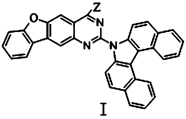
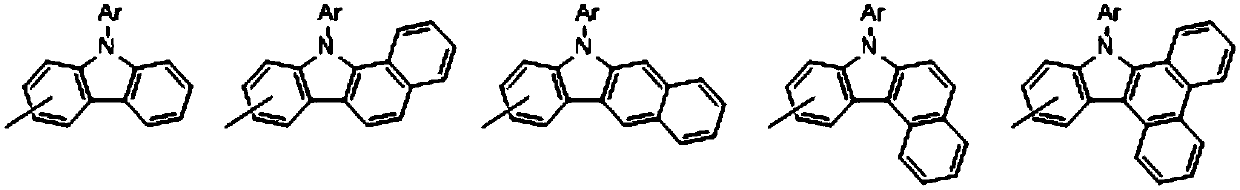
Phosphorescent compound and organic light emitting diode device using same
A compound and phosphorescence technology, applied in luminescent materials, organic chemistry, electric solid devices, etc., can solve the problems of complex manufacturing process, low process efficiency, and lack of solubility, and achieve excellent color purity and brightness, and prolong durability.
- Summary
- Abstract
- Description
- Claims
- Application Information
AI Technical Summary
Problems solved by technology
Method used
Image

Examples
no. 1 approach
[0087] The ITO glass substrate was patterned to have a light emitting area of 3 mm x 3 mm. Then, the patterned ITO glass substrate was washed.
[0088] The substrate is then placed in a vacuum chamber. The standard pressure setting is 1×10 -6 support. After that, on the ITO substrate with
[0089] with The sequence forms layers of organic matter.
[0090] At 0.9mA, the brightness is equal to 1224cd / m 2 (5.9V). At this time, CIEx=0.659, y=0.331.
no. 2 approach
[0092] The ITO glass substrate was patterned to have a light emitting area of 3 mm x 3 mm. Then, the patterned ITO glass substrate was washed.
[0093] The substrate is then placed in a vacuum chamber. The standard pressure setting is 1×10 -6 support. After that, on the ITO substrate with
[0094] with The sequence forms layers of organic matter.
[0095]At 0.9mA, the brightness is equal to 1142cd / m 2 (6.1V). At this time, CIEx=0.660, y=0.330.
no. 3 approach
[0097] The ITO glass substrate was patterned to have a light emitting area of 3 mm x 3 mm. Then, the patterned ITO glass substrate was washed.
[0098] The substrate is then placed in a vacuum chamber. The standard pressure setting is 1×10 -6 support. After that, on the ITO substrate with
[0099] with The sequence forms layers of organic matter.
[0100] At 0.9mA, the brightness is equal to 1203cd / m 2 (6.0V). At this time, CIEx=0.658, y=0.330.
PUM
| Property | Measurement | Unit |
|---|---|---|
| luminance | aaaaa | aaaaa |
| luminance | aaaaa | aaaaa |
Abstract
Description
Claims
Application Information