Analog enhancement method for image contrast

A technology for enhancing image and contrast, applied in image communication, parts of color TV, parts of TV system, etc., can solve problems such as loss of precision, loss, and inability to output, and achieve the effect of high resolution

Active Publication Date: 2019-04-26
BEIJING SUPERPIX MICRO TECHNOLOGY CO LTD
View PDF11 Cites 2 Cited by
  • Summary
  • Abstract
  • Description
  • Claims
  • Application Information

AI Technical Summary

Problems solved by technology

However, due to the amplification in the digital domain, there will be a problem of loss of precision. For example, ADC_OUT is 100 and 101, and after digital enhancement and amplification, it is 400 and 404. Obviously, the digital signals 401, 402, and 403 in the middle are lost and cannot output

Method used


Image

  • Analog enhancement method for image contrast
  • Analog enhancement method for image contrast
  • Analog enhancement method for image contrast

Examples


Embodiment Construction

[0021] The technical solutions in the embodiments of the present invention will be clearly and completely described below in conjunction with the accompanying drawings in the embodiments of the present invention. Obviously, the described embodiments are only some of the embodiments of the present invention, not all of them. Based on the embodiments of the present invention, all other embodiments obtained by persons of ordinary skill in the art without making creative efforts belong to the protection scope of the present invention.

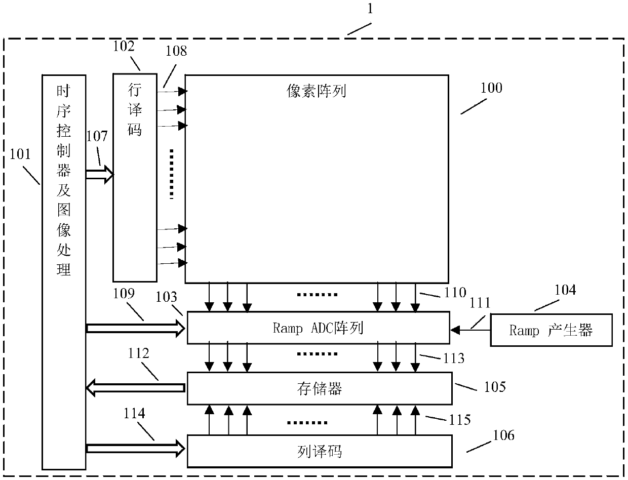
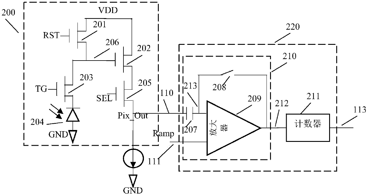
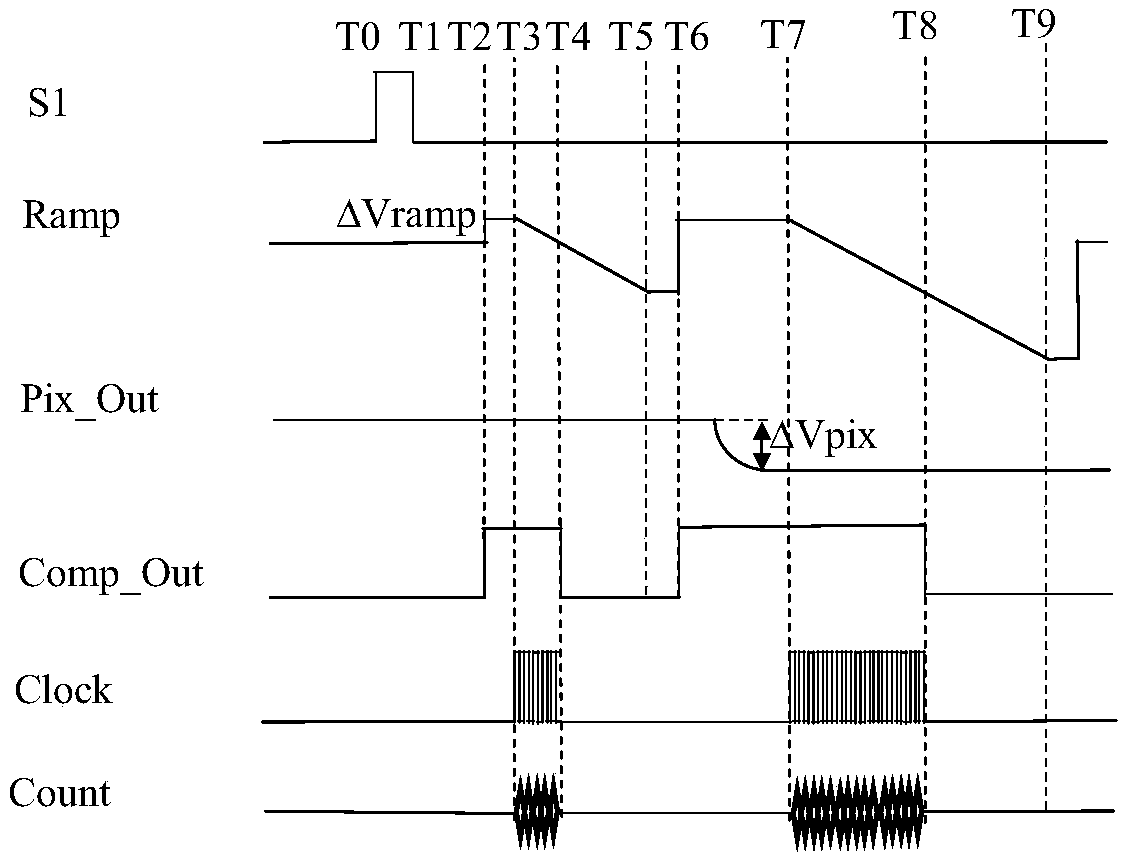
[0022] The embodiment of the present invention provides a method for simulating and enhancing the contrast of an image. The Ramp generator is used to output the Ramp signal of the divided area, and the contrast is increased by an analog circuit. By adjusting the area division and the corresponding slope adjustment (adjusting the analog gain by area), To realize the amplification and reduction of the signal. This method can be applied to figure 1 T...


PUM


Abstract

The invention discloses an analog enhancement method for image contrast. The method includes the following steps: adopting a Ramp generator to output a Ramp signal of a partitioned region, and adopting the way of increasing the contrast by using an analog circuit to implement the amplification and reduction of the signal through regional division adjustment and corresponding slope adjustment, wherein the implementation of signal amplification includes the following process: adjusting the regional division and the corresponding slope to realize the amplification of a concerned signal region, and adjusting the slope to realize the reduction of a non-concerned signal region. The method adopts the way of increasing the contrast by using the analog circuit, and realizes the amplification and reduction of the signals by adjusting the analog gain in different regions; and since the operation is performed before ADC quantization, the loss of accuracy cannot occur, and the resolution of imagescan be higher.

Description

technical field [0001] The invention relates to the technical fields of CMOS (Complementary Metal-Oxide-Semiconductor) image sensor imaging and the like, and in particular to a method for simulating and enhancing image contrast. Background technique [0002] CMOS image sensors are widely used in many fields such as electronic consumption, security monitoring, automatic control, medical treatment and national defense. [0003] figure 1 It is a schematic diagram of a CMOS image sensor with a column Ramp ADC structure. The CMOS image sensor 1 with a column Ramp ADC structure includes a pixel array 100 , a timing control and image processor 101 , a row decoder 102 , a Ramp ADC array 103 , a Ramp generator 104 , a memory 105 , and a column decoder 106 . Wherein the pixel array 100 is composed of a pixel unit 200 (see the pixel unit example figure 2 ) to form an array, the Ramp ADC array 103 is composed of Ramp ADC 220 (see the example of Ramp ADC figure 2 ) to form an array...

Claims


Application Information

Patent Timeline
Patent Type & Authority Applications(China)
IPC IPC(8): H04N5/374H04N5/3745
CPCH04N25/772H04N25/76
Inventor 李文杰旷章曲
Owner BEIJING SUPERPIX MICRO TECHNOLOGY CO LTD
Why Eureka
Try Eureka