Heterojunction tunneling field-effect transistor and its preparation method

A tunneling field effect and heterojunction technology, applied in semiconductor devices, electrical components, circuits, etc., can solve the problem of increasing the leakage current of two-dimensional material heterojunction TFET

Active Publication Date: 2021-05-18
HUAWEI TECH CO LTD
View PDF5 Cites 0 Cited by
  • Summary
  • Abstract
  • Description
  • Claims
  • Application Information

AI Technical Summary

Problems solved by technology

[0005] The embodiment of the present application provides a heterojunction tunneling field-effect transistor and its preparation method, which are used to solve the problem that there are no dangling bonds on the surface of the two-dimensional material in the foregoing solution, but there are still dangling bonds at the boundary of the material, and the dangling bonds will increase the two-dimensional The Leakage Current Problem of Material Heterojunction TFET

Method used


Image

  • Heterojunction tunneling field-effect transistor and its preparation method
  • Heterojunction tunneling field-effect transistor and its preparation method
  • Heterojunction tunneling field-effect transistor and its preparation method

Examples


Embodiment Construction

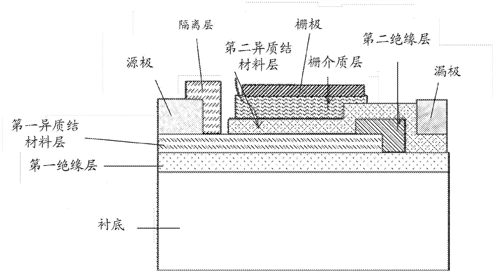
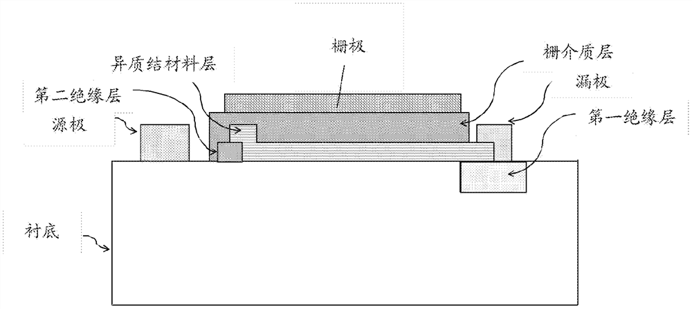
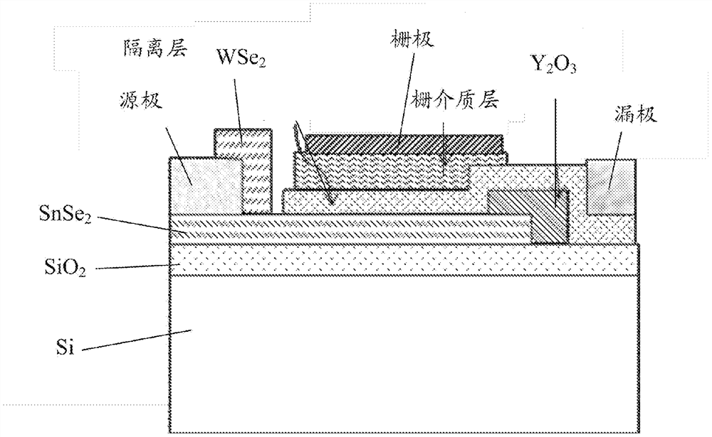
[0081] In order to overcome the problem that there is no dangling bond on the surface of the two-dimensional material in the commonly used TFET, but there are still dangling bonds on the boundary of the material, and the dangling bond will increase the leakage current of the two-dimensional material heterojunction TFET. One-dimensional materials are transferred to bulk materials to form heterojunctions or two two-dimensional materials are stacked to form heterojunctions. An oxide layer is grown on the edge of the material at the junction region of the heterojunction (that is, the overlapping region of the two materials), and the edge It is a solution to isolate the edge and increase the tunneling distance of carriers at the edge to reduce the tunneling leakage current. The structure and preparation method of the heterojunction tunneling field effect transistor provided in this application will be described in detail below.

[0082] The heterojunction region of the heterojuncti...


PUM


Abstract

An embodiment of the present application provides a heterojunction tunneling field effect transistor and a manufacturing method thereof, comprising: a first insulating layer covering the upper surface of the substrate, and a first heterojunction material layer covering the upper surface of the first insulating layer One end of the source is arranged on the top, the source is arranged on one end of the first heterojunction material layer, a second insulating layer is arranged around the other end of the first heterojunction material layer, and the isolation layer is arranged on the heterojunction layer, The isolation layer covers the inner side of the source electrode; the second heterojunction material layer covers the other end of the first heterojunction material layer, the second insulating layer, and the second insulating layer, forming a heterojunction with the first heterojunction material layer. material junction, the drain is arranged on the other end of the second heterojunction layer opposite to the source; the gate dielectric layer covers the position between the source and the drain on the second heterojunction material layer, and the gate is arranged on on the gate dielectric layer. By setting the second insulating layer for isolation, the leakage current caused by the edge state is significantly reduced, and a heterojunction is formed by using two-dimensional materials, which avoids interface defects caused by lattice mismatch.

Description

technical field [0001] The embodiments of the present application relate to semiconductor technology, and in particular to a heterojunction tunneling field-effect transistor (TunnelField-Effect Transistors, TFET for short) and a manufacturing method thereof. Background technique [0002] Integrated circuits continue to shrink according to Moore's Law, but when the size of transistors enters the 14nm and 10nm nodes, the size of transistors is further reduced, and the leakage current caused by the short-channel effect continues to increase, causing the power consumption of integrated circuits to become an increasingly serious problem . Unlike traditional Metal-Oxide-Semiconductor Field-Effect Transistor (Metal-Oxide-Semiconductor Field-Effect Transistor, referred to as: MOSFET) working mechanism is different, tunneling field effect transistor TFET adopts the band-to-band tunneling mechanism, and its subthreshold slope (Subthreshold Slope, Abbreviation: SS) can be lower than t...

Claims


Application Information

Patent Timeline
IPC IPC(8): H01L29/78H01L29/10
CPCH01L29/10H01L29/78
Inventor 李伟徐挽杰徐慧龙张臣雄
Owner HUAWEI TECH CO LTD
Why Eureka
Try Eureka