Memorizer and forming method thereof

A memory and substrate technology, applied in the direction of electric solid devices, semiconductor devices, electrical components, etc., can solve the problems of high resistance of the common source contact, high filling stress of all tungsten, affecting the performance of the memory, etc., so as to avoid structural changes. , The effect of improving isolation performance and reducing power consumption

Active Publication Date: 2019-05-10
YANGTZE MEMORY TECH CO LTD
View PDF5 Cites 44 Cited by
  • Summary
  • Abstract
  • Description
  • Claims
  • Application Information

AI Technical Summary

Problems solved by technology

However, there are currently the following problems: the stress of full tungsten filling is too high, which will greatly affect the subsequent manufacturing process; although polysilicon a

Method used


Image

  • Memorizer and forming method thereof
  • Memorizer and forming method thereof
  • Memorizer and forming method thereof

Examples


Embodiment Construction

[0024] The specific implementation of the memory provided by the present invention and its forming method will be described in detail below in conjunction with the accompanying drawings.

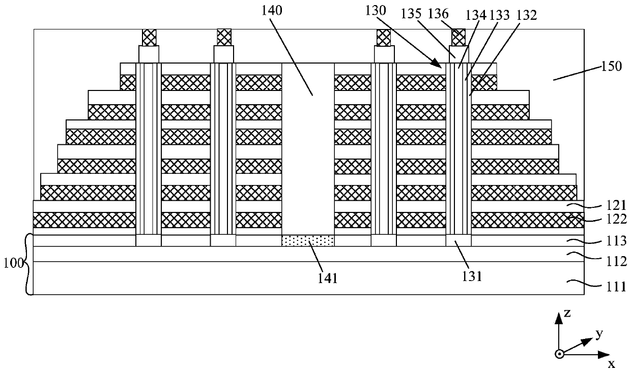
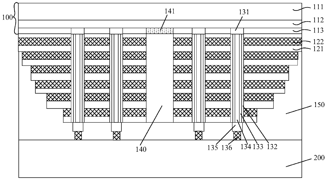
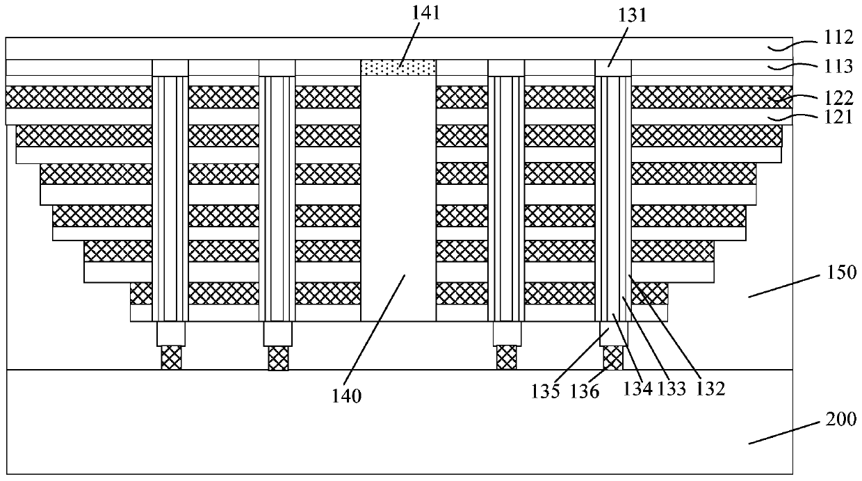
[0025] Please refer to figure 1 , providing a storage substrate, the storage substrate includes: a substrate 100 and a storage stack structure formed on the front surface of the substrate; a channel column structure 130 penetrating to the surface of the substrate is also formed in the storage stack structure, a penetrating The isolation wall 140 from the initial stack structure to the surface of the substrate; a common source doped region 141 is formed in the substrate 100 at the bottom of the isolation wall 140 .

[0026] The substrate 100 may be a semiconductor material, such as a single crystal silicon substrate, a single crystal germanium substrate, an SOI (silicon on insulator) substrate or a GOI (germanium on insulator) substrate, etc., and the substrate 100 may also be For n-type do...


PUM


Abstract

The invention relates to a memorizer and a forming method thereof. The forming method of the memorizer comprises the following steps: providing a memory base, wherein the memory base comprises a substrate and a memory stack structure formed on the front of the substrate, a channel column structure and an isolation wall, which penetrate through the memory stack structure to a surface of the substrate, are formed in the memory stack structure, and a common source doped area is formed in the substrate at the bottom of the isolation wall; thinning the back of the substrate; forming a medium layerat the back of the thinned substrate; etching the medium layer and forming an opening, wherein the opening exposes the common source doped area in the substrate; filling the opening with a conductivelayer, and connecting to the common source doped area, wherein the conductive layer is used as a common source contact part. The method provided by the invention is beneficial for improving performance of the memorizer.

Description

technical field [0001] The invention relates to the technical field of semiconductors, in particular to a memory and a forming method thereof. Background technique [0002] In recent years, the development of flash memory (Flash Memory) is particularly rapid. The main feature of flash memory is that it can keep stored information for a long time without power on, and has the advantages of high integration, fast access speed, easy erasing and rewriting, etc. Has been widely used. In order to further increase the bit density (Bit Density) of the flash memory while reducing the bit cost (Bit Cost), three-dimensional flash memory (3D NAND) technology has been developed rapidly. [0003] 3D NAND memory, including a substrate and a memory stack structure formed on the surface of the substrate. The memory stack structure is formed with a channel column structure penetrating to the surface of the substrate to form a vertically arranged memory string. The bottom of the memory strin...

Claims


Application Information

Patent Timeline
IPC IPC(8): H01L27/1157H01L27/11582
CPCH10B43/35H10B43/27
Inventor 刘毅华刘峻范鲁明
Owner YANGTZE MEMORY TECH CO LTD
Why Eureka
Try Eureka