Single-grid control voltage current sampling device based on LIGBT

A technology for controlling voltage and current sampling, which is applied to electrical components, semiconductor devices, circuits, etc., can solve the problems that current sampling and voltage sampling cannot be performed at the same time, and cannot fully meet high-voltage applications, so as to achieve controllable sampling ratio and sampling accuracy high effect

Active Publication Date: 2019-05-10
UNIV OF ELECTRONIC SCI & TECH OF CHINA
View PDF7 Cites 4 Cited by
  • Summary
  • Abstract
  • Description
  • Claims
  • Application Information

AI Technical Summary

Problems solved by technology

However, this structure cannot have the functions of current sampling and voltage sampli

Method used


Image

  • Single-grid control voltage current sampling device based on LIGBT
  • Single-grid control voltage current sampling device based on LIGBT
  • Single-grid control voltage current sampling device based on LIGBT

Examples


Example Embodiment

[0029] Example 1

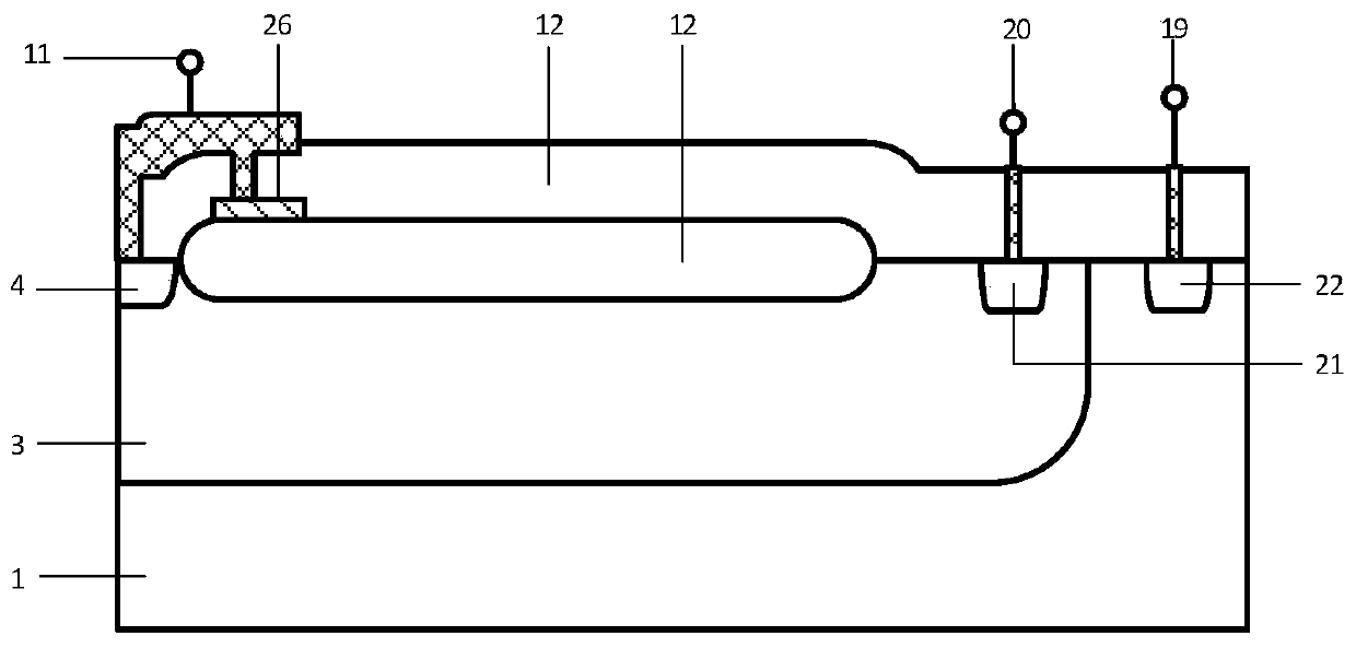
[0030] A single-gate control voltage and current sampling device based on LIGBT of the present invention, such as image 3 As shown, the cell structure includes a first conductivity type semiconductor substrate 1 and a substrate electrode 19 located on the lower surface of the first conductivity type semiconductor substrate 1; the upper surface of the first conductivity type semiconductor substrate 1 has an epitaxial oxide layer 2. The upper surface of the epitaxial oxide layer 2 has a second conductivity type semiconductor drift region 3; the second conductivity type semiconductor drift region 3 has a second conductivity type semiconductor doped region 4; the second conductivity type semiconductor doped The miscellaneous region 4 has a first conductivity type semiconductor anode region 5, the upper surface of the first conductivity type semiconductor anode region 5 has a first metal electrode 11; the second conductivity type semiconductor drift region 3 has a f...

Example Embodiment

[0038] Example 2

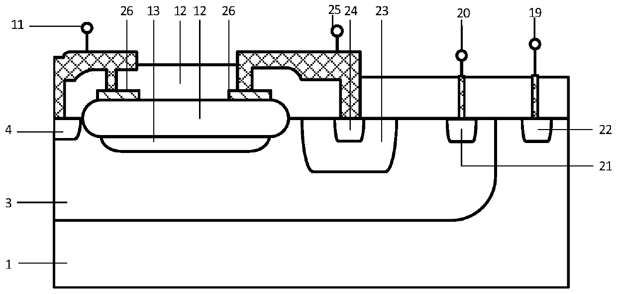
[0039] Such as Figure 4 As shown, the difference between this embodiment and Embodiment 1 is that the second conductivity type semiconductor doped region 7, the first conductivity type semiconductor doped region 8, and the second conductivity type semiconductor doped region 7 are sequentially arranged on the right side of the second conductivity type semiconductor cathode region 6 A conductive type semiconductor cathode region 9; a gap is provided between the right side of the second conductive type semiconductor cathode region 6 and the second conductive type semiconductor doped region 7, the second conductive type semiconductor doped region 7 and the first conductive type semiconductor The doped regions 8 are arranged next to each other.

Example Embodiment

[0040] Example 3

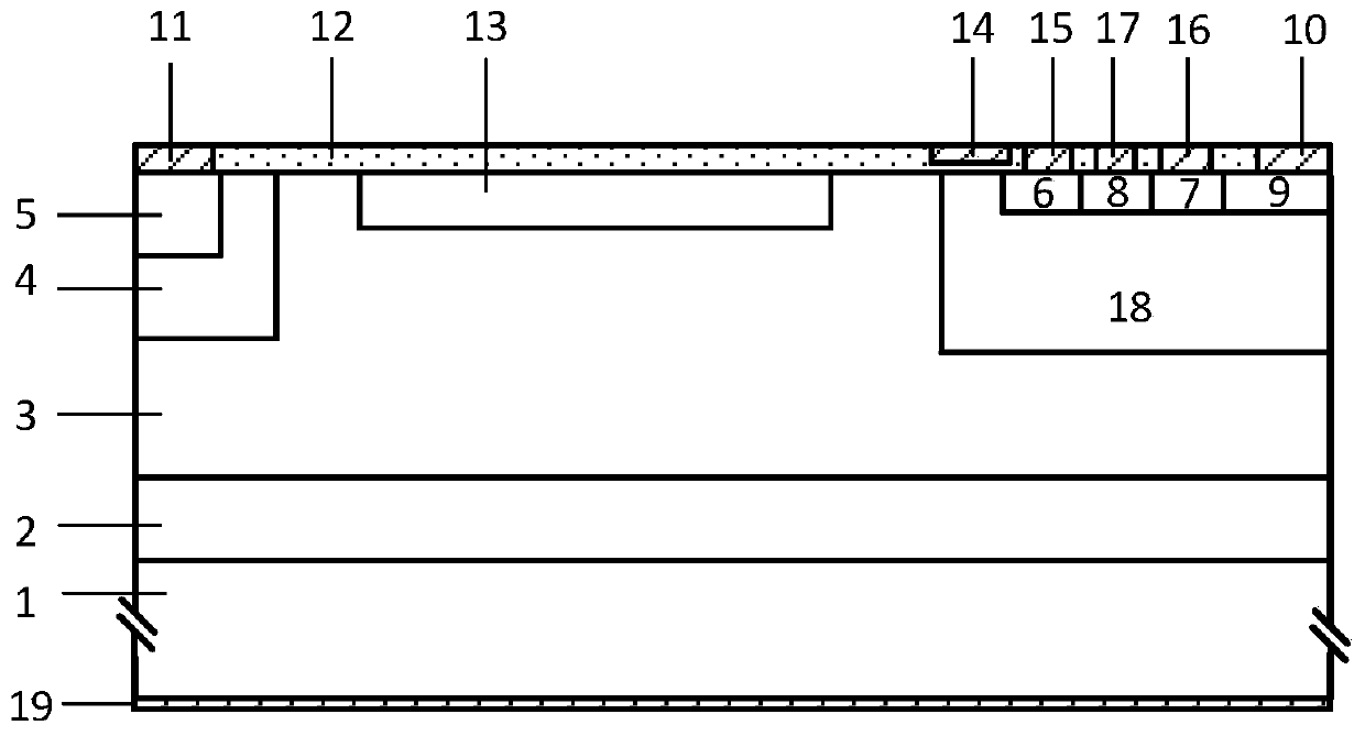
[0041] Such as Figure 5 As shown, the difference between this embodiment and Embodiment 1 lies in that: the first conductivity type semiconductor cathode region 9 and the second conductivity type semiconductor doped region 7 are arranged on the right side of the second conductivity type semiconductor cathode region 6 in sequence. Doped region 8; the second conductivity type semiconductor doped region 7 and the first conductivity type semiconductor doped region 8 are immediately arranged.


PUM


Abstract

The invention provides a single-grid control voltage current sampling device based on LIGBT. A cellular structure thereof comprises a first conductive type semiconductor substrate, a substrate electrode, an epitaxial oxide layer, a second conductive type semiconductor drift region, a second conductive type semiconductor doping area, a first conductive type semiconductor anode region, a first metalelectrode, a first conductive type semiconductor area, an oxide layer, a metal grid, a first conductive type semiconductor doping area, a second conductive type semiconductor cathode area, a first conductive type semiconductor doping area, a second conductive type semiconductor doping area, a first conductive type semiconductor cathode area, a third metal electrode, a fourth metal electrode, a fifth metal electrode, and a second metal electrode. The device can sample the current flowing through the device at a switch-on state, the detection on the anode voltage can be realized at the off transient, the current sampling and the voltage sampling are alternately performed, the sampling precision is high, and the sampling ratio is controllable.

Description

technical field [0001] The invention belongs to the technical field of power semiconductor devices, and relates to a LIGBT-based single gate control voltage and current sampling device. Background technique [0002] In the high-voltage, power integrated circuits and systems related to power drives, it is necessary to detect the input / output performance and load conditions of high-voltage and power integrated circuits, so as to achieve real-time protection of circuits and systems and meet the intelligence of integrated circuits and systems. It can effectively ensure the normal and reliable operation of the system. Realizing the control of high-voltage and power integrated circuits and their application systems is a research hotspot and scientific difficulty at home and abroad. [0003] Power semiconductor devices face many failures in practical applications, such as short-circuit events and transient current peak overshoots under inductive loads. The damage of devices in a s...

Claims


Application Information

Patent Timeline
IPC IPC(8): H01L29/739
Inventor 李泽宏杨洋彭鑫赵一尚程然何云娇
Owner UNIV OF ELECTRONIC SCI & TECH OF CHINA
Why Eureka
Try Eureka