Super-junction device and manufacturing method thereof

A super-junction device, N-type technology, applied in semiconductor/solid-state device manufacturing, semiconductor devices, electrical components, etc., can solve problems affecting BVds, affecting P-N balance, and reducing the ability of the terminal area to withstand lateral voltage

Active Publication Date: 2019-05-14
SHENZHEN SANRISE TECH CO LTD
View PDF8 Cites 1 Cited by
  • Summary
  • Abstract
  • Description
  • Claims
  • Application Information

AI Technical Summary

Problems solved by technology

But the problem is that even if the N-type epitaxial layer is made into two layers, the concentration of the upper half is high, and the concentration of the lower half is low, but in this way, there will still be significantly more N-type impurities than P-type impurities in the bottom area of ​​the trench. P-N balance, thus affecting BVds
Another problem is that due to the increase in the concentration of the N-type epitaxy at the top of the terminal region, the ability of the terminal region to withstand voltage laterally is reduced, resulting in device breakdown occurring in the terminal region, which not only fails to improve the effect of BVds, but also due to BVds Occurs at the terminal, making the consistency of BVds worse, and the EAS capability of the device is also worse

Method used


Image

  • Super-junction device and manufacturing method thereof
  • Super-junction device and manufacturing method thereof
  • Super-junction device and manufacturing method thereof

Examples


no. 1 example approach

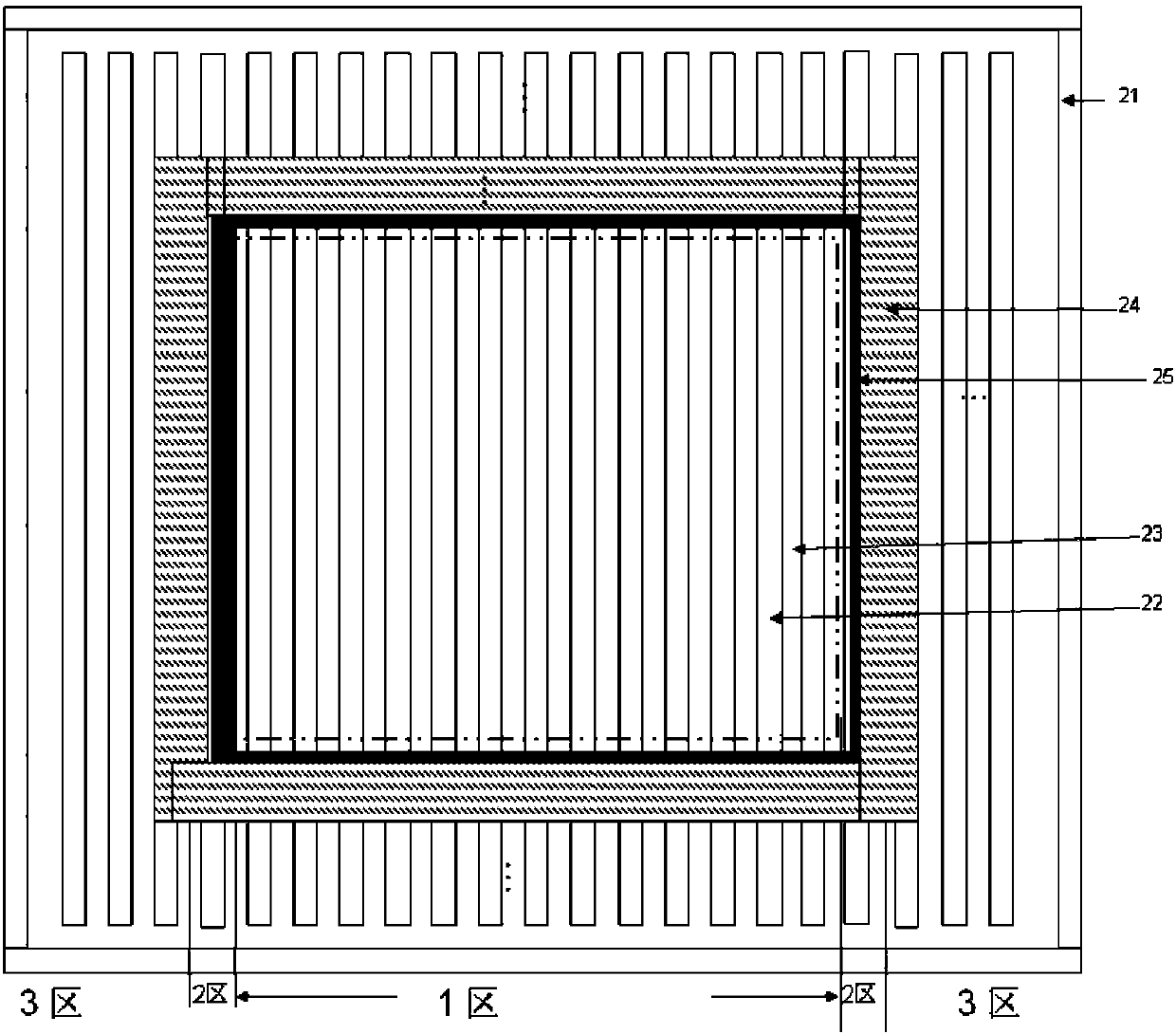
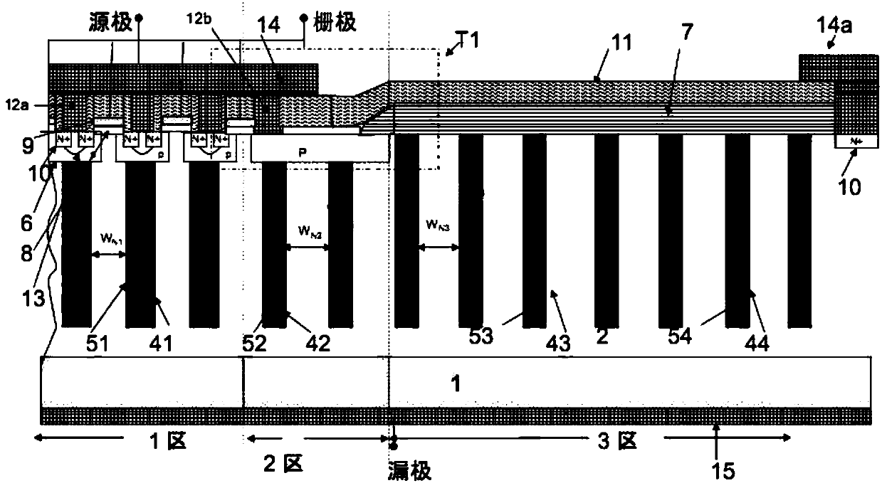
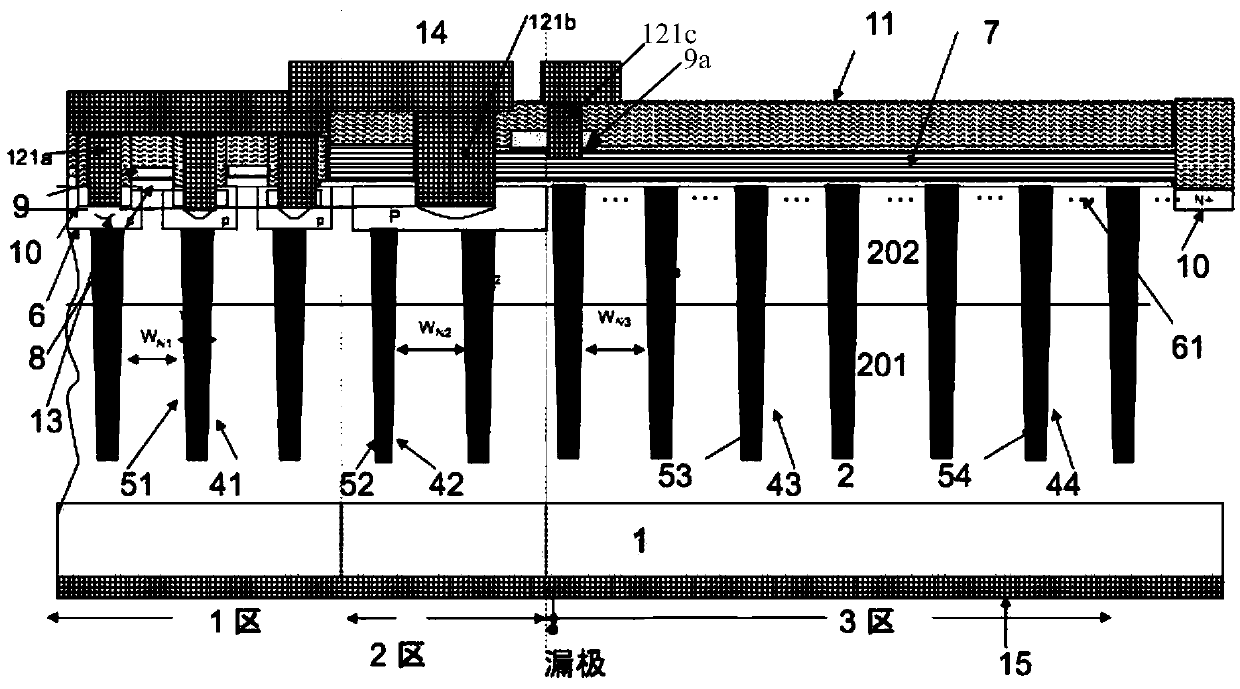
[0132] The manufacturing method of the super junction device according to the first embodiment of the present invention is to manufacture such as image 3 The superjunction device of the embodiment of the present invention is shown as an example for description, as Figure 5A to Figure 5H Shown is a schematic cross-sectional view of the device in each step of the manufacturing method of the super-junction device in the first embodiment of the present invention; in the manufacturing method of the super-junction device in the first embodiment of the present invention, the middle region of the super-junction device is the current flow region, that is, 1 zone, the terminal zone, that is, zone 3, surrounds the periphery of the current flow region, and the transition zone, that is, zone 2, is located between the current flow zone and the terminal zone; the structure of the top view of the super junction device can also refer to figure 1 shown. The method of the first embodiment of ...


PUM


Abstract

The invention discloses a super-junction device. A groove of the super-junction structure is of a side face inclined structure; the doping concentration of an N-type epitaxial layer is of a step distribution structure; a P-type column is composed of a P-type ion implantation region formed at the bottom of the groove, and a P-type epitaxial layer which are arranged in a stacked mode; a protective ring oxide film surrounds the peripheral side of a current flow region; and the N-type epitaxial layer at the oxide film epitaxial layer interface of the N-type epitaxial layer in the protective ring oxide film and a terminal region comprises a top region with lowered N type doping concentration, so that the transverse depletion capability of the N-type column at the interface of the epitaxial layer of the oxidation film can be enhanced. The invention further discloses a manufacturing method of the super-junction device. According to the invention, the charge balance between the P-type column and the N-type column of the super-junction structure with the inclined groove can be improved, the longitudinal voltage withstand capability of the device is improved, and the source and drain breakdown voltage of the device is improved; and the capacity of bearing transverse voltage of the device terminal can be improved, and the reliability of the device can be improved.

Description

technical field [0001] The invention relates to a method for manufacturing a semiconductor integrated circuit, in particular to a method for manufacturing a superjunction device. Background technique [0002] The super junction structure is composed of alternately arranged N-type pillars and P-type pillars. If the superjunction structure is used to replace the N-type drift region in the vertical double-diffused MOS transistor (Vertical Double-diffused Metal-Oxide-Semiconductor, VDMOS) device, the conduction path is provided through the N-type column in the conduction state, and when the conduction The P-type column does not provide a conduction path; in the off state, the PN column jointly bears the reverse bias voltage, forming a super-junction metal-oxide-semiconductor field-effect transistor (Metal-Oxide-Semiconductor Field-Effect Transistor, MOSFET). The super-junction MOSFET can greatly reduce the on-resistance of the device by using a low-resistivity epitaxial layer w...

Claims


Application Information

Patent Timeline
Patent Type & Authority Applications(China)
IPC IPC(8): H01L29/78H01L29/06H01L21/336
Inventor 肖胜安
Owner SHENZHEN SANRISE TECH CO LTD
Why Eureka
Try Eureka