A kind of semiconductor material preparation equipment

A semiconductor and equipment technology, applied in the field of semiconductor material preparation equipment, can solve the problems of complex experimental instruments, difficult to control variables, and large equipment footprint, and achieve the effects of reducing floor space, increasing efficiency, and increasing accuracy

Active Publication Date: 2021-05-25
托特半导体(山东)有限公司
View PDF7 Cites 0 Cited by
  • Summary
  • Abstract
  • Description
  • Claims
  • Application Information

AI Technical Summary

Problems solved by technology

The current production of lanthanum-calcium-manganese-oxygen thin films by spin-coating must be carried out manually, and there are problems such as complex experimental instruments, many required equipment and large floor area, easy introduction of impurities by manual operation, and difficulty in controlling variables caused by differences in experimental techniques. Therefore, It is necessary to propose a kind of semiconductor material preparation equipment that has automatic operation, saves space, and is more convenient for scientific research and control variables.

Method used


Image

  • A kind of semiconductor material preparation equipment
  • A kind of semiconductor material preparation equipment
  • A kind of semiconductor material preparation equipment

Examples


Embodiment Construction

[0044] The following will clearly and completely describe the technical solutions in the embodiments of the present invention with reference to the accompanying drawings in the embodiments of the present invention. Obviously, the described embodiments are only some, not all, embodiments of the present invention. Based on the embodiments of the present invention, all other embodiments obtained by persons of ordinary skill in the art without making creative efforts belong to the protection scope of the present invention.

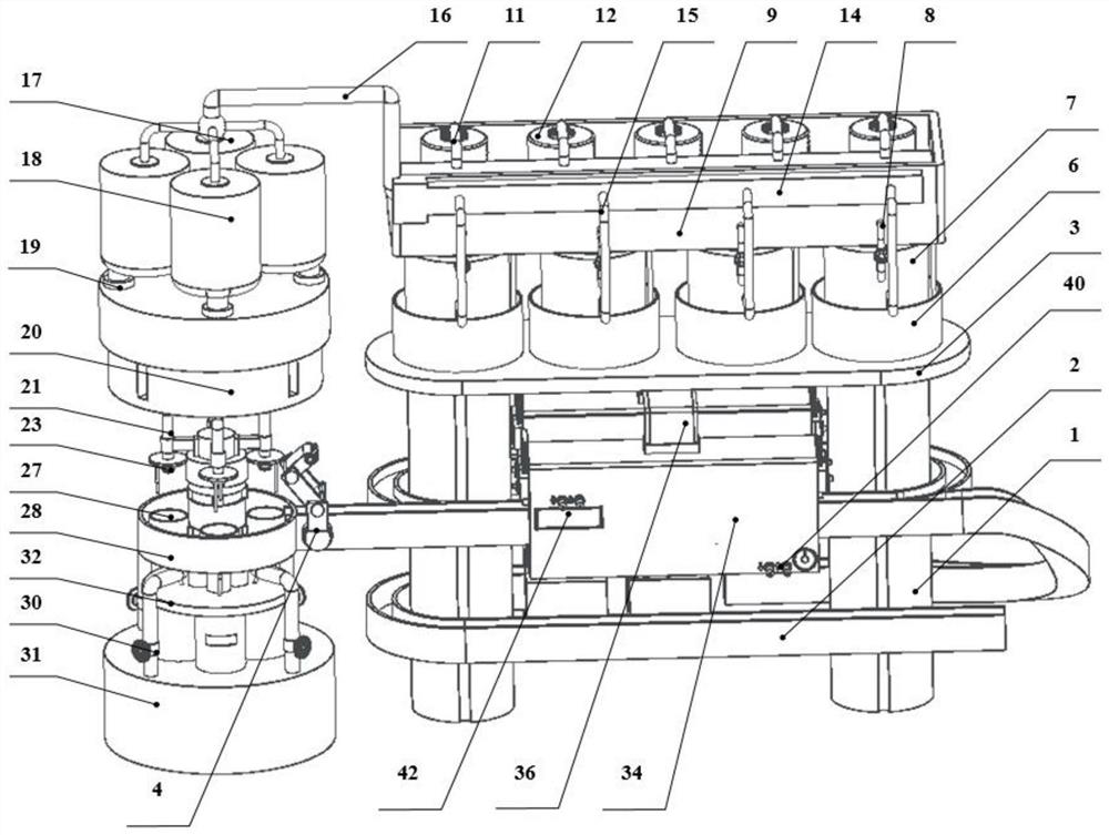
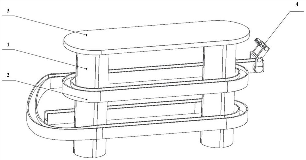
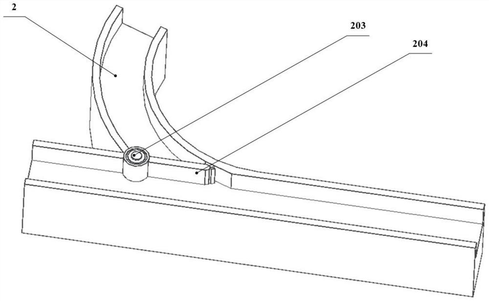
[0045] Such as Figure 1-20 Shown: A kind of semiconductor material preparation equipment, including base frame conveying system, sol system, spin coating system, sintering system, testing system, base frame conveying system, spin coating system are set on the same horizontal plane, sol system is fixedly set on the base frame Above the conveying system, the sintering system and testing system are set at different heights inside the base frame conveying system,...


PUM


Abstract

The invention relates to a semiconductor material preparation equipment. A base frame transmission system, a sol system, a spin coating system, a sintering system, and a testing system are arranged on the same horizontal plane, and the sol system is fixedly arranged on the base frame to convey Above the system, the sintering system and testing system are set at different heights inside the base frame transmission system, and the base frame transmission system passes through the sintering system and the test system in turn; the invention has the function of automatic operation; it is equipped with a three-layer vertical structure, which can effectively Reduce the footprint of the equipment and increase the scope of use of the equipment; compound semiconductor thin films can be prepared, which further strengthens the scientific research use of the invention, and at the same time the electromagnetic performance test of the thin film can be carried out; multiple times of mixing in the sample preparation can make the The colloid is fully homogenized.

Description

technical field [0001] The invention relates to a material preparation device, in particular to semiconductor material preparation equipment. Background technique [0002] At present, doped perovskite manganese oxide La 1-x A x MnO 3 (A=Ca, Ba, Sr) semiconductors have special electronic transport and magnetic properties, and have received a lot of attention, and are widely used in photoelectric fast devices, magnetic sensors, spin valve devices and giant magnetoresistance sensors. In devices such as bolometers. The current production of lanthanum-calcium-manganese-oxygen thin films by spin-coating must be carried out manually, and there are problems such as complex experimental instruments, many required equipment and large floor area, easy introduction of impurities by manual operation, and difficulty in controlling variables caused by differences in experimental techniques. Therefore, It is necessary to propose a kind of semiconductor material preparation equipment tha...

Claims


Application Information

Patent Timeline
Patent Type & Authority Patents(China)
IPC IPC(8): G01N1/28G01N1/38G01N1/42G01N1/44G01N27/72G01D21/02
Inventor 李松和刘军李明霞
Owner 托特半导体(山东)有限公司
Why Eureka
Try Eureka