Photosensitive imaging detection chip based on tip electron fluorescence excitation and preparation method thereof

A photosensitive imaging and chip technology, which is applied in photometry, photometry using electric radiation detectors, optical radiation measurement, etc., to achieve the effects of improved detection sensitivity, high detection sensitivity, fast response and spectral conversion

Active Publication Date: 2019-05-21
NANJING OPY ELECTRONICS TECH CO LTD
View PDF4 Cites 1 Cited by
  • Summary
  • Abstract
  • Description
  • Claims
  • Application Information

AI Technical Summary

Problems solved by technology

[0004] In view of the above defects or improvement needs of the prior art, the present invention provides a photosensitive imaging detection chip based on cutting-edge electronic fluorescence excitation and its preparation method, the purpose of which is to solve the above-mentioned technical problems existing in the existing photosensitive imaging array, and The photosensitive imaging detection chip based on

Method used


Image

  • Photosensitive imaging detection chip based on tip electron fluorescence excitation and preparation method thereof
  • Photosensitive imaging detection chip based on tip electron fluorescence excitation and preparation method thereof
  • Photosensitive imaging detection chip based on tip electron fluorescence excitation and preparation method thereof

Examples


Example Embodiment

[0051] In order to make the objectives, technical solutions and advantages of the present invention clearer, the following further describes the present invention in detail with reference to the accompanying drawings and embodiments. It should be understood that the specific embodiments described herein are only used to explain the present invention, but not to limit the present invention. In addition, the technical features involved in the various embodiments of the present invention described below can be combined with each other as long as they do not conflict with each other.

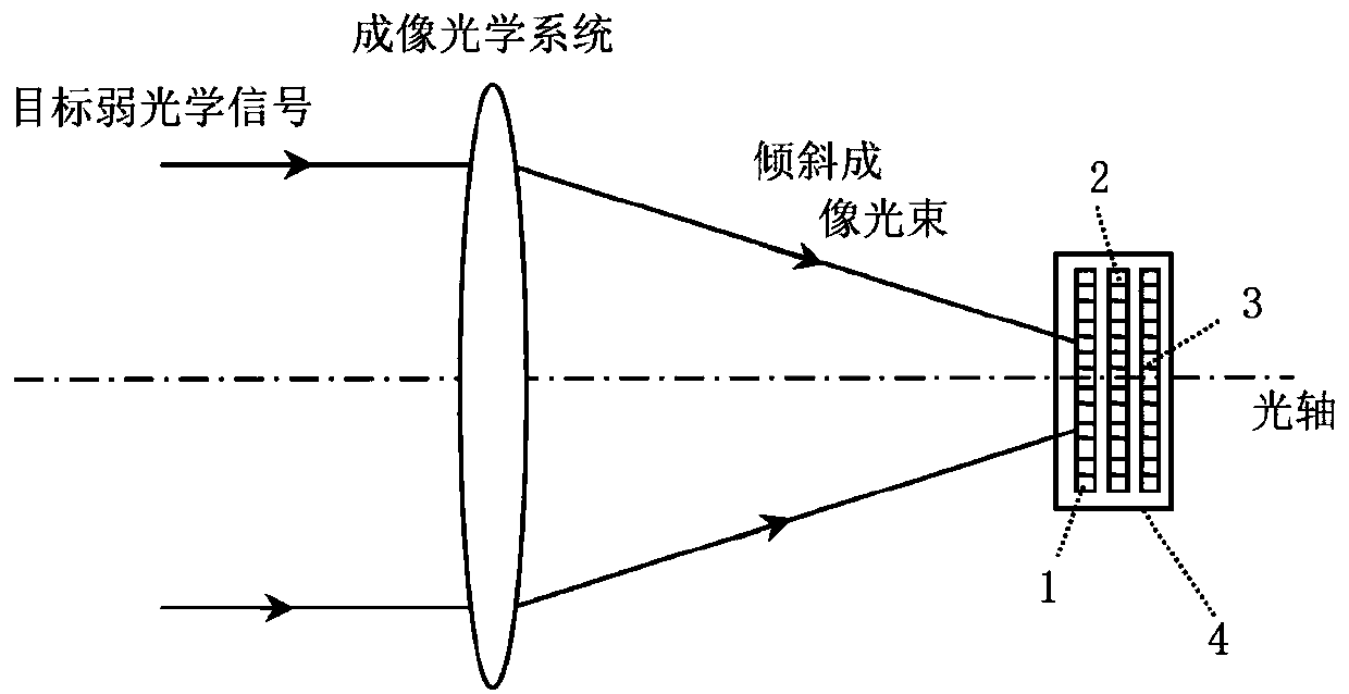
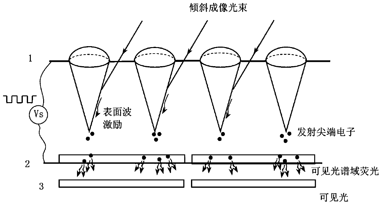
[0052] On the surface of a variety of functional materials (such as conventional metals or semiconducting silicon germanium, etc.), the effect of resonant surface waves can be generated by visible light or infrared light radiation; surface waves composed of surface electromagnetic waves and surface electron density waves Or surface plasmons, the effective transport distance on the surface of functional...


PUM

PropertyMeasurementUnit
Diameteraaaaaaaaaa

Abstract

The invention discloses a photosensitive imaging detection chip based on tip electronic fluorescence excitation. The photosensitive imaging detection chip comprises an optical antenna, a fluorescent film layer and a photosensitive array which are arranged in parallel, wherein the optical antenna is of an array structure composed of a plurality of antenna elements which are arranged at intervals and electrically connected. The fluorescent film layer is of an array structure composed of a plurality of fluorescent film elements which are arranged at intervals and electrically connected. The photosensitive array is of an array structure composed of a plurality of photosensitive elements which are arranged at intervals. The optical antenna, the fluorescent film layer and the photosensitive array are the same in shape and array scale, the antenna elements of the optical antenna, the fluorescent film elements at the corresponding positions in the fluorescent film layer and the photosensitiveelements at the corresponding positions in the photosensitive array are aligned with one another in the vertical direction, and each antenna element of the optical antenna comprises at least one nanopointed cone of which the top surfaces are electrically connected with one another. Incident light amplification and conversion from infrared light to visible light spectrum are realized through electron controlled emission and fluorescence excitation of the nano pointed cones, so that the detection sensitivity is remarkably improved.

Description

technical field [0001] The invention belongs to the technical field of optical imaging detection, and more specifically relates to a photosensitive imaging detection chip based on cutting-edge electronic fluorescence excitation and a preparation method thereof. Background technique [0002] At present, photosensitive imaging arrays, as photosensitive detectors, have been widely used in various fields. Common photosensitive imaging arrays include photon detectors and thermal detectors, and photon detectors include visible light detectors (commonly CMOS devices) and infrared detectors (commonly FPAs). Visible light detectors are mainly used in the civilian field, and the minimum detectable optical power is as low as nanowatts; infrared detectors are mainly used in the military field, and their cost is relatively high; thermal detectors are based on micro-heat absorption and photoelectric signal generation This thermal detection mode works. [0003] However, there are some te...

Claims


Application Information

Patent Timeline
IPC IPC(8): G01J1/02G01J1/42
Inventor 张新宇张汤安苏
Owner NANJING OPY ELECTRONICS TECH CO LTD
Why Eureka
Try Eureka