Method for detecting surface contamination of silicon wafer

A silicon wafer surface and detection method technology, applied in the direction of measuring devices, material analysis through optical means, instruments, etc., can solve the problem that it is impossible to determine what kind of substance the silicon wafer pollutants are

Inactive Publication Date: 2019-05-21
GCL POLY ENERGY HLDG
View PDF9 Cites 4 Cited by
  • Summary
  • Abstract
  • Description
  • Claims
  • Application Information

AI Technical Summary

Problems solved by technology

[0004] Based on this, it is necessary to provide a method for detecting silicon wafer surface contamination that can determine what kind of substance the pollutants in the contaminated area on the silicon wafer surface are for the problem that it is impossible to determine what kind of substance the pollutants in the contaminated area on the silicon wafer surface are.

Method used


Image

  • Method for detecting surface contamination of silicon wafer
  • Method for detecting surface contamination of silicon wafer
  • Method for detecting surface contamination of silicon wafer

Examples


Embodiment 1

[0054] A method for detecting contamination on the surface of a polysilicon wafer, comprising the steps of:

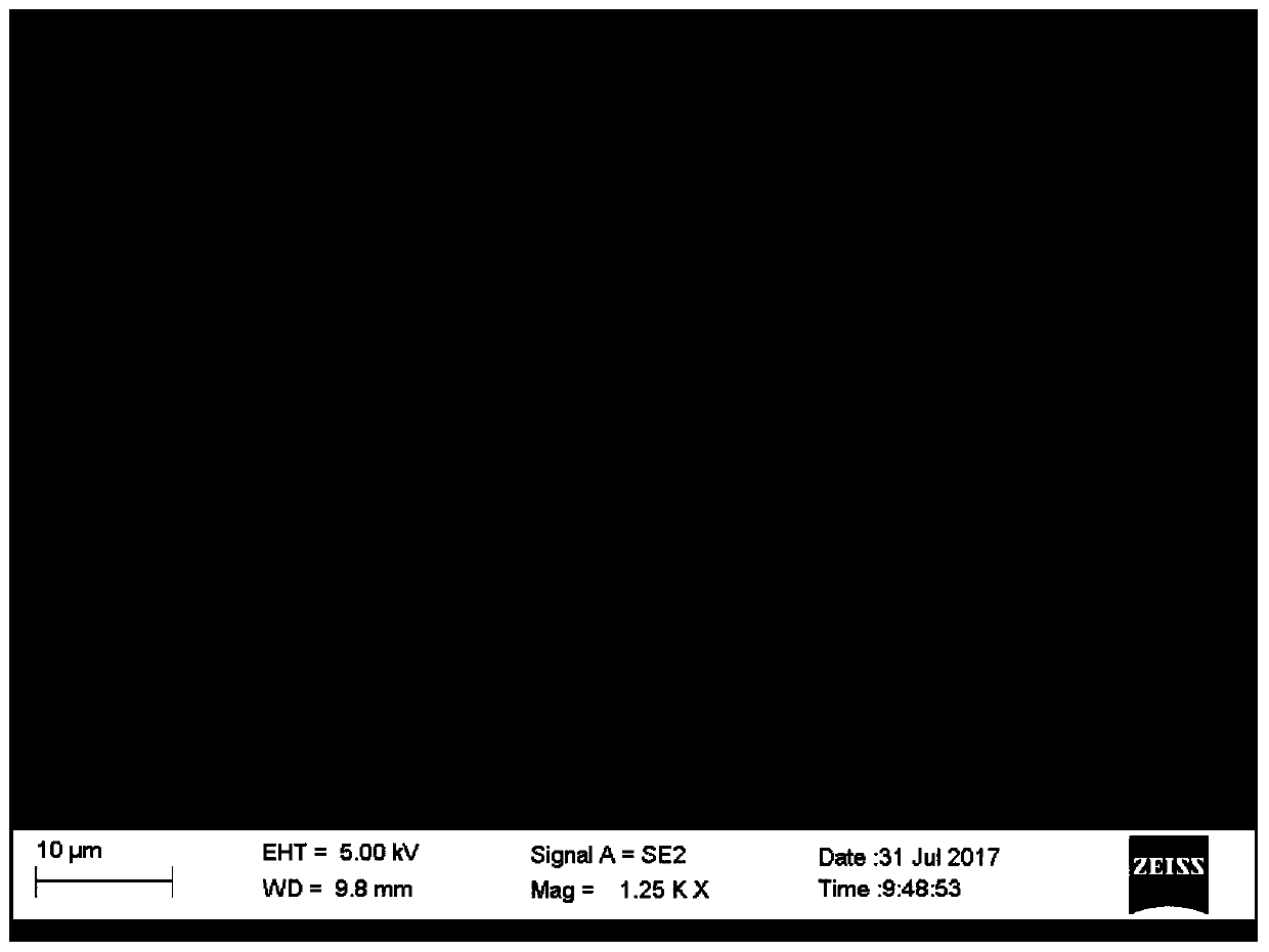
[0055] 1. Adhere the polysilicon wafer sample on the sample stage, and then put the polysilicon wafer sample together with the sample stage into the sample chamber of the scanning electron microscope, and evacuate to 2.0×10 -5 mbar, then adjust the electron beam acceleration voltage to 5kV, and the magnification is 1250 times, scan the contaminated area on the surface of the polysilicon wafer sample, and obtain the microscopic image of the contaminated area, see figure 1 .

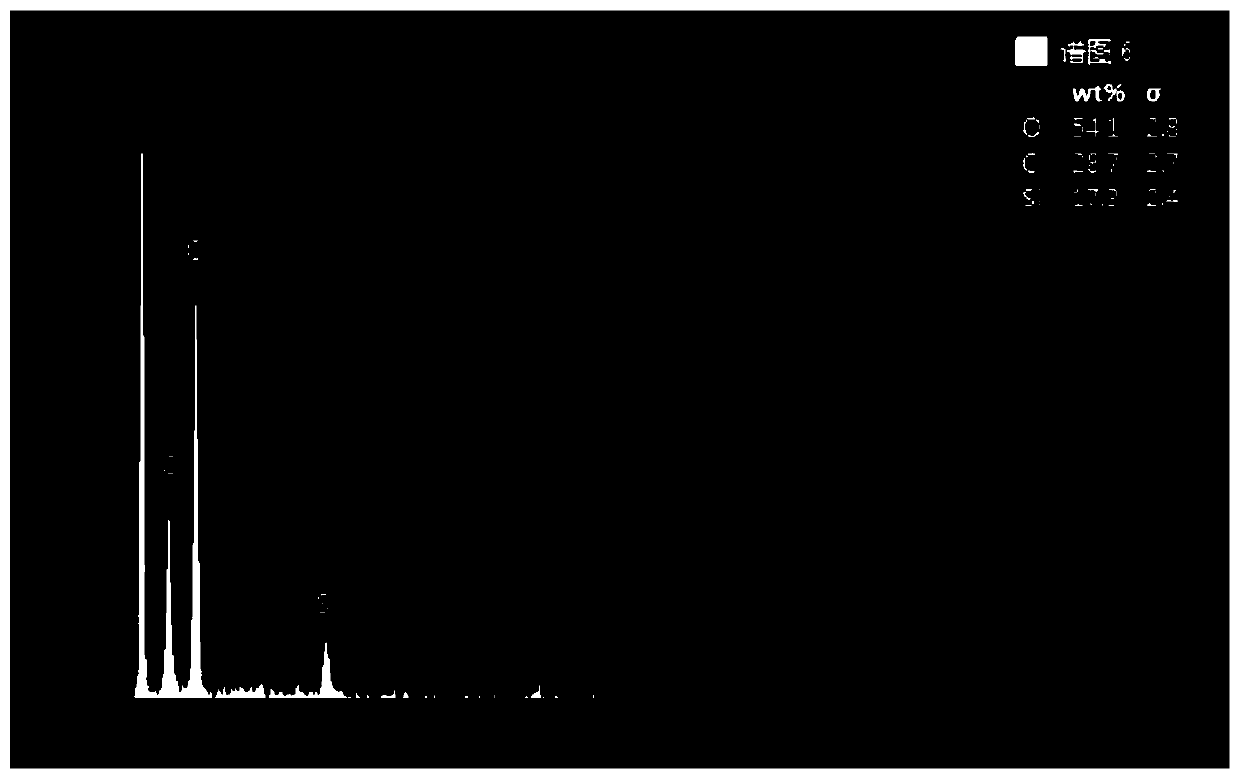
[0056] 2. Adjust the electron beam acceleration voltage to 20kV, and the X-ray energy spectrum analyzer collects the X-ray energy spectrum signals of the contaminated area, and confirms that the contaminated area contains three elements, C, O and Si, see figure 2 .

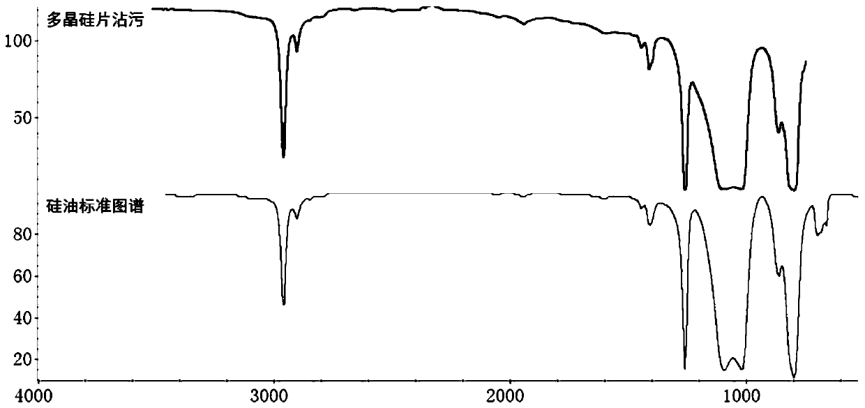
[0057] 3. Transfer the polysilicon wafer sample to the stage of the micro-infrared spectrometer, and collect the micro-infrared sp...

Embodiment 2

[0060] A method for detecting contamination on the surface of a single crystal silicon wafer, comprising the steps of:

[0061] 1. Adhere the monocrystalline silicon wafer sample on the sample stage, and then put the monocrystalline silicon wafer sample together with the sample stage into the sample chamber of the scanning electron microscope, and evacuate to 2.0×10 -5 mbar, then adjust the electron beam acceleration voltage to 5kV, and the magnification is 200 times, scan the contaminated area on the surface of the single crystal silicon wafer sample, and obtain the microscopic image of the single crystal contaminated area.

[0062] 2. Adjust the electron beam acceleration voltage to 20kV, and the X-ray energy spectrum analyzer collects the X-ray energy spectrum signal of the contaminated area, and confirms that the contaminated area contains two elements, C and O.

[0063] 3. Transfer the single crystal silicon wafer sample to the stage of the micro-infrared spectrometer, an...


PUM

PropertyMeasurementUnit
thicknessaaaaaaaaaa

Abstract

The invention relates to a method for detecting surface contamination of a silicon wafer. The method comprises the steps: performing a composition analysis on a contaminated area to determine an elemental composition of a contaminant in the contaminated area; and collecting an infrared spectrum of the contaminated area and comparing the infrared spectrum of the contaminated area with an infrared spectrum of a standard sample library. According to the provided method, the specific object of the contaminant in the contaminated area on the silicon wafer surface can be determined comprehensively;and the specific components of the contaminant in the contaminated area on the silicon wafer surface can be determined qualitatively by combining the elemental composition of the contaminant in the contaminated area of the silicon wafer surface and the comparison of the infrared spectrum of the contaminated area with the standard map. Therefore, the method has the great significance in determiningthe contamination source and checking and the cause of contamination.

Description

technical field [0001] The invention relates to the field of silicon chip contamination detection, in particular to a detection method for silicon chip surface contamination. Background technique [0002] With the continuous upgrading of photovoltaic industry technology, more stringent requirements are put forward for the process standards of crystalline silicon solar cells. As the main body of crystalline silicon solar cells, silicon wafers have a crucial impact on the quality of photovoltaic modules. [0003] Surface contamination of silicon wafers is one of the most common defects in the production process of silicon wafers. Since the contamination of silicon wafers is usually very small, and the pollutants have different shapes and complex components, it is difficult to judge the pollutants on the surface of silicon wafers empirically. What kind of substance. Traditional methods for analyzing the composition of pollutants on the surface of silicon wafers mainly include...

Claims


Application Information

Patent Timeline
Patent Type & Authority Applications(China)
IPC IPC(8): G01N21/3563G01N23/2251
Inventor 吉鑫阮文娟
Owner GCL POLY ENERGY HLDG
Why Eureka
Try Eureka