

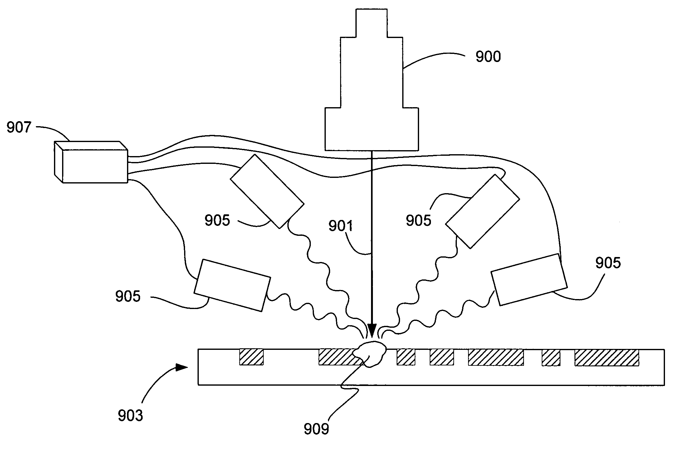
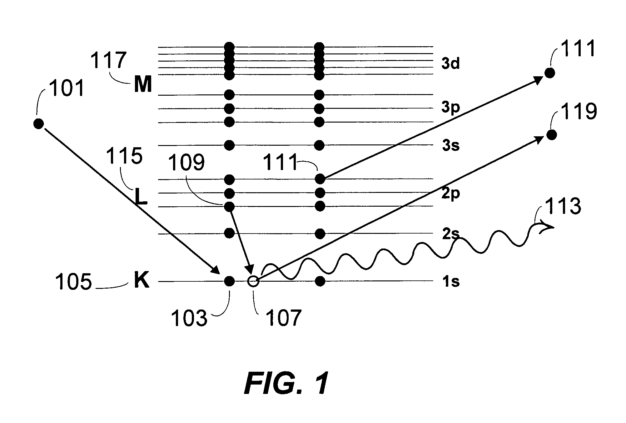
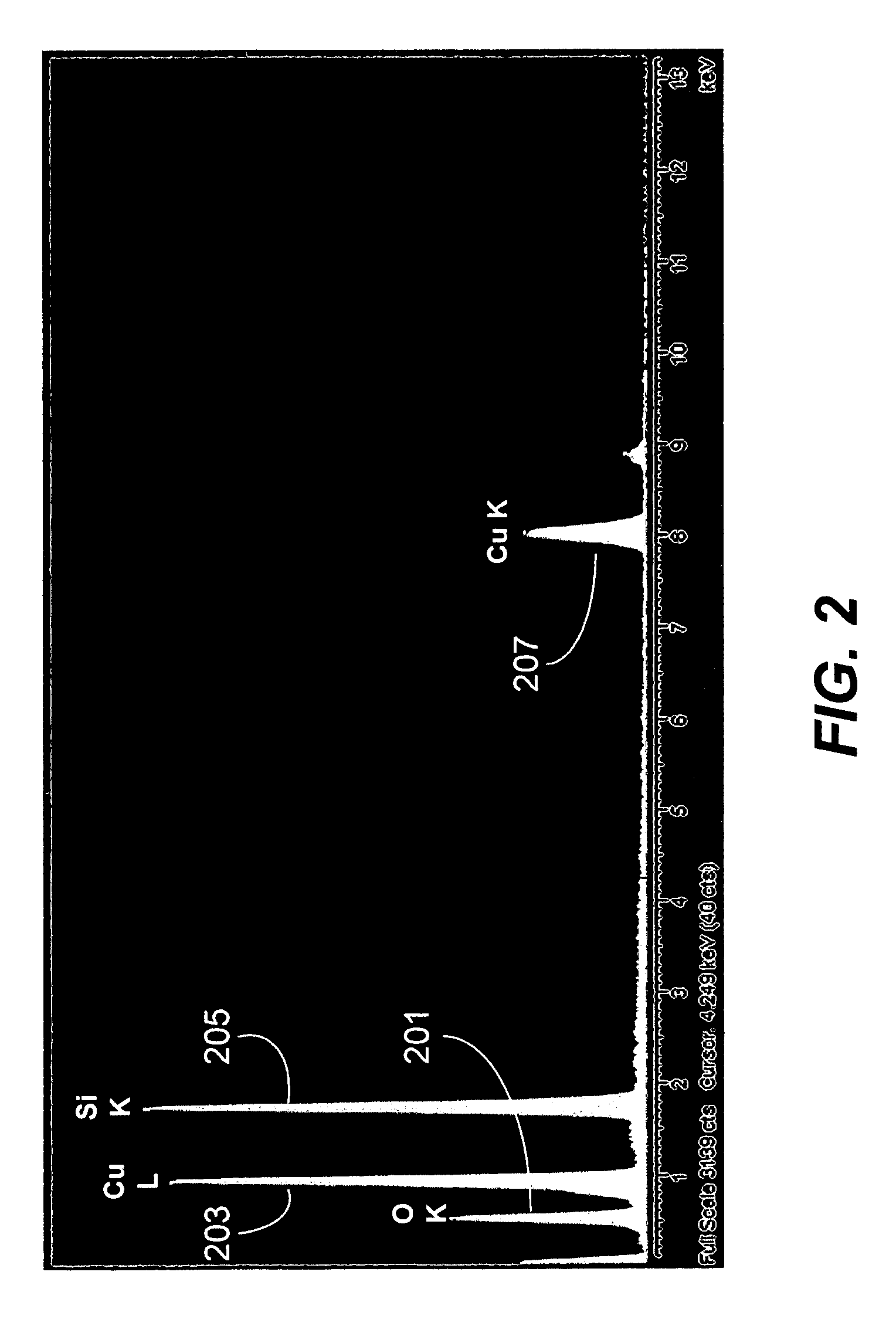
Rapid defect composition mapping using multiple X-ray emission perspective detection scheme
a defect composition and detection scheme technology, applied in the field of semiconductor device inspection, can solve the problems of scratch defect, structural flaw, residual process material and other surface contamination, etc., and achieve the effect of improving the confidence of spatially resolved data
- Summary
- Abstract
- Description
- Claims
- Application Information
AI Technical Summary
Benefits of technology
Problems solved by technology
Method used
Image

Examples
Embodiment Construction
[0032]Introduction
[0033]In the following description, numerous specific details are set forth in order to provide a thorough understanding of the present invention. The present invention may be practiced without some or all of these specific details. In other instances, well known process operations have not been described in detail to not unnecessarily obscure the present invention. While the invention will be described in conjunction with the specific embodiment, it will be understood that it is not intended to limit the invention to the embodiment. On the contrary, it is intended to cover alternatives, modifications, and equivalents as may be included within the spirit and scope of the invention as defined by the appended claims.
[0034]A “semiconductor wafer” or “wafer” is a semiconductor substrate at any state of manufacture in the production of integrated circuits. One standard semiconductor wafer described in this invention is 200 mm in diameter, 0.75 mm thick (see e.g., SEMI S...
PUM
 Abstract
Description
Claims
Application Information